
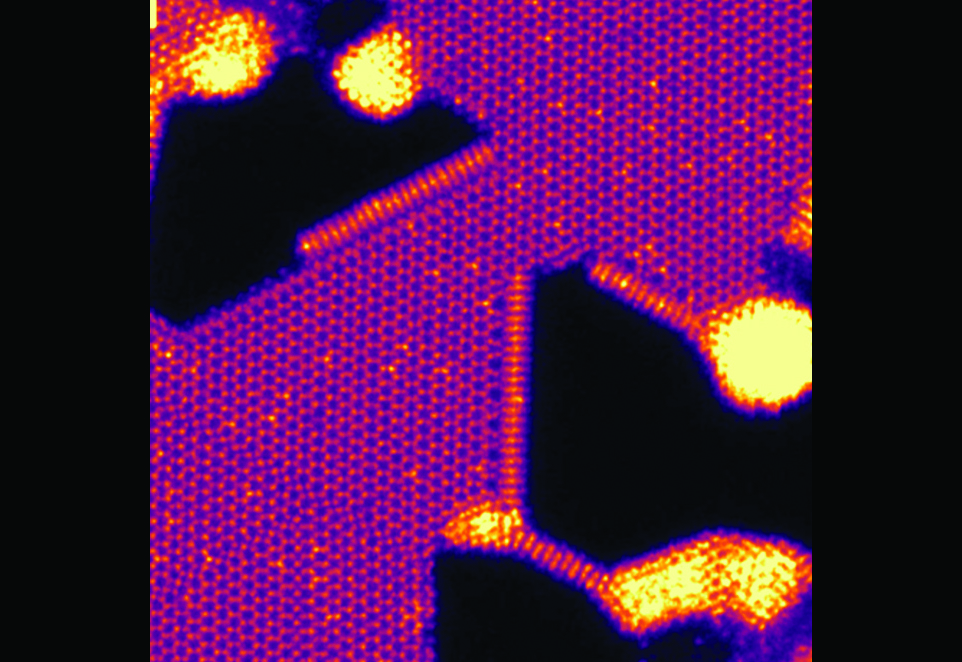
August 1, 2018 – An Oak Ridge National Laboratory–led team has learned how to engineer tiny pores embellished with distinct edge structures inside atomically-thin two-dimensional, or 2D, crystals. The 2D crystals are envisioned as stackable building blocks for ultrathin electronics and other advanced devices, but their edges and pores are especially reactive for catalysis, sensing or separations functions. Their formation and structure had not been well understood to date. Using a heating microchip inside a scanning transmission electron microscopy at ORNL’s Center for Nanophase Materials Sciences, the scientists induced changes in the local chemical environment of a 2D material to reveal the atomic rearrangements leading to the formation of different nanopore edges. Theorists’ predictions from thermodynamics explained the four stable configurations that formed most often. “Before, we had to take whatever we got from a materials’ synthesis,” said ORNL’s Xiahan Sang. “Now we can be proactive at creating edges.” The work was published in Nature Communications.


