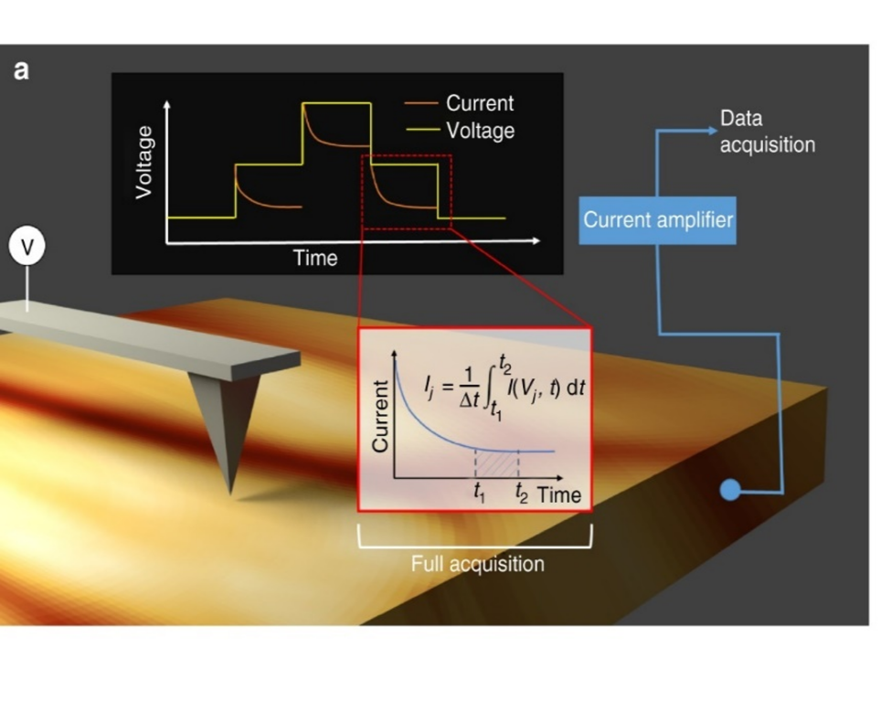
Conductive Atomic Force Microscopy (C-AFM) is a powerful technique that extends beyond the imaging capabilities of traditional AFM by allowing for the direct measurement of electrical conductivity across a sample's surface at the nanoscale. This method involves a conductive tip that not only senses topographical features but also detects local electrical currents, providing a unique blend of morphological and electrical insights.
The basic setup involves a conductive AFM tip biased relative to a grounded bottom electrode. Current that flows through the tip-sample interface is detected and amplified using a high-gain current amplifier, with the amplified signal then fed into a data acquisition system for analysis. C-AFM is invaluable for the detailed investigation of conductive pathways, junction characteristics, and local defect states in a wide array of materials and devices, including semiconductors, metals, insulators, and nanocomposites.
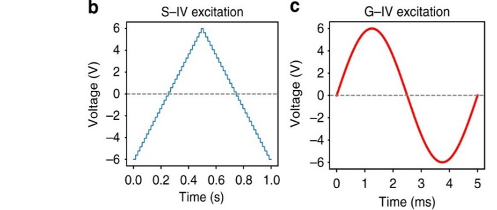
IV Spectroscopy involves measuring the current-voltage (I-V) characteristics of a material or device, providing information on its electronic structure, charge transport mechanisms, and defect levels. This method is crucial for understanding the fundamental electrical behavior, including resistance, capacitance, and semiconducting properties, of various systems ranging from single molecules to complex semiconductor devices.
General Mode IV (G-IV), on the other hand, offers a broader and more flexible approach to electrical characterization. It allows the rapid acquisition of I-V curves under various conditions or modes, potentially including different environmental conditions, frequencies, or illumination levels. G-IV can reveal detailed insights into the dynamic electrical responses of materials, facilitating the study of phenomena such as photoconductivity, frequency-dependent conductivity, and more complex charge transport behaviors.
Features
Available modes:
- C-AFM imaging
- IV-Spectroscopy
- G-Mode IV
Specifications
- Current ranges: 100 fA to 10 nA, 1nA to 10 uA,
- Sample up to buffer size
- Automatized large stage motion.
- Scan range (100x100 um)
- Z height limit (<10 µm)
- Band Excitation Imaging and Spectroscopies
- FPGA Scanner Control
- PyAE workflows
Applications
- Semiconductors
- Microelectronics
- Photovoltaics
- Energy storage
- Corrosion and material degradation
- Ionic materials
Equipment
- Cypher AFM, MFP3D AFM (Asylum Research) in ambient
- Icon Dimension (Bruker) in ambient
- Icon Dimension (Bruker) in Ar glovebox
- Drive AFM (Nanosurf) in ambient
References
Somnath, S., Law, K.J.H., Morozovska, A.N. et al. Ultrafast current imaging by Bayesian inversion. Nature Communications 9, 513 (2018).
Contacts

Ionic conductivity, IV spectroscopy
Nano and Microelectronics and devices

Electronic and domain walls conductivity, IV spectroscopy