As the size of electronic devices continues to shrink, it becomes more challenging to measure their electrical properties using traditional techniques. AFM provides a solution to this problem by enabling the measurement and local modification of electrical/electrochemical properties at the nanoscale. Voltage or bias modulated AFM is a powerful tool for investigating a wide range of electrostatic, electrical, electronic, and ionic properties of materials and surfaces.
To perform these electrical measurements, specialized tips are required. Typically, a conventional silicon AFM cantilever is coated with an electrically conductive material to act as a probe. These tips can be used to measure a wide range of electrical properties, including conductivity, resistance, and capacitance. In addition to providing electrical property data, VM-AFM can also simultaneously provide topographical information. This means that the technique can be used to investigate the relationship between electrical properties and surface topography, which is important in many applications. AFM has numerous applications in the field of electronics, including the characterization of nanoscale devices such as transistors, memory devices, and sensors. It can also be used to investigate the properties of materials used in electronic devices, such as thin films, coatings, and semiconductors.
What do we mean by electrical, electronic, and ionic?
- Electrical properties generally refer to the fundamental electrical characteristics of materials, such as resistivity, conductivity, and dielectric constant. These properties relate to the ability of a material to conduct or resist the flow of electrical current and are determined by the nature of the material's atomic structure, composition, and other intrinsic factors (Probed by C-AFM, Quantitative EFM)
- Electronic properties, on the other hand, refer specifically to the behavior of electrons in materials and devices, including their movement and interactions with other electrons and with external stimuli such as electrical or magnetic fields. Electronic properties include characteristics such as band structure, carrier mobility, and recombination rates, which determine the efficiency and performance of electronic devices (Probed by KPFM, SIMIM)
- Ionic properties refer to the behavior and movement of charged particles (ions) in materials and solutions. Important ionic properties include ionic conductivity, diffusion coefficient, and mobility. These properties are crucial for optimizing the performance and efficiency of various applications, including electrochemistry, battery technology, fuel cells, and biosensors. The presence of ions can also affect other properties, such as electrical conductivity, surface charge, and electrochemical potential. (Probed by TR-KPFM, EcFM, ESM)
Operation Modes
Conductive AFM (C-AFM)
Conductive atomic force microscopy (C-AFM) is a current sensing AFM mode that simultaneously measures the topography of a material (via force feedback) and the electric current flow through the tip-sample junction. C-AFM utilizes a sharp, conductive probe to map local variations in a sample's electrical properties (e.g. conductivity, IV) with nanoscale resolution.
As the probe scans the surface, a bias voltage is applied between the AFM tip and the sample, and the resulting current flow is measured with a low noise, high gain preamplifier. The collected current signal is used to create a 2D map of conductivity.
C-AFM is commonly used to study a sample's conductivity and image electrical properties such as charge transport and charge distribution on the nanoscale. It is widely used in the fields of nanoelectronics, solar cell, and semiconductor industries for conducting high-resolution measurements. These measurements include semiconductor dopant profiling, as well as quality control for dielectric films and oxide layers.
Electrical Force Microscopy (EFM)
Both EFM and KPFM are non-destructive, surface-sensitive techniques that allow mapping of various electronic/electrochemical properties with high lateral resolution (tens of nanometers). These properties include work function distributions (for metals or semiconductors), surface charge or surface potential distributions (for insulators), and dielectric properties. Both techniques use a biased vibrating AFM probe to scan the sample surface, measuring electrostatic forces.
The EFM method typically involves driving a conductive probe with an AC voltage, which forms a capacitor between the tip and sample that accumulates electrostatic energy. The resulting electrostatic force is proportional to the capacitance gradient of the probe-sample system and can be measured locally by the tip. The modulated tip voltages result in spectral components, including a DC force component (Fdc), a force at the modulation frequency (Fω), and a force at double the frequency (F2ω) of the tip voltage. The amplitude and phase of these dynamic channels are captured using traditional lock-in amplifier detection.
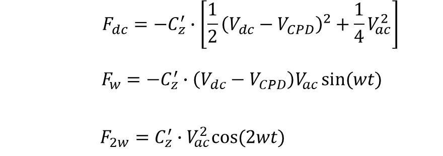
In frequency-modulated EFM, the resonant excitation is maintained by adjusting the driving frequency, and the frequency shift is collected as the EFM image. The force gradient can also be described and measured in a similar fashion to the forces above.
The main difference between the EFM and KPFM techniques is that KPFM involves bias voltage feedback, which enables the direct measurement of absolute work function values of the sample. Therefore, KPFM is considered a quantitative approach, while EFM is considered qualitative. However, under certain conditions it is possible to quantify local properties, including dielectric constants, from the EFM signal (see dielectric spectroscopy)
Kelvin Probe Force Microscopy (KPFM)
KPFM is a technique based on the macroscopic “Kelvin probe” which was developed to measure the contact potential difference (CPD) between two dissimilar metals. In the case of KP, this is achieved by applying an external potential to a metal probe or sample until the current or surface charges between the two are nullified. This equilibrated state represents the CPD or work function difference (∆Φ) between the metals.
A major drawback to current detection used in the macroscopic Kelvin probes is an ultimate limit on the size with which the probes can be decreased to before sensitivity deteriorates. So, while the scanning Kelvin probe is a quantitative approach, it lacks sufficient spatial resolution as compared to EFM. At the same time, while EFM allows spatial resolution on much smaller scales, it is largely a qualitative method. Not long after the realization of EFM, a few researchers had the idea to combine the best elements of EFM with the macroscopic Kelvin method.
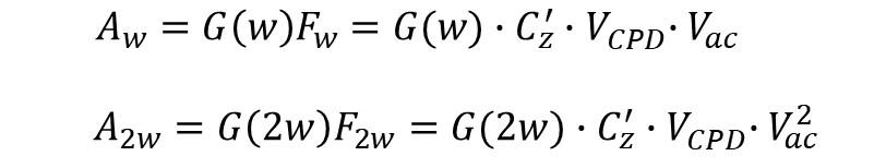
Simple schematic describing an (a) AM- and (b) FM-KPFM experimental setup. Reprinted from (Collins, 2018, ROPP)
Double pass KPFM
The initial demonstration of KPFM utilized amplitude modulated detection in a dual pass or lift mode. In this scheme, shown in Figure X, topography is captured during the first line trace with the cantilever mechanically vibrating. On the lift scan, the probe is electrostatically excited by the tip bias (Vtip) without mechanical excitation. The driving frequency of the AC voltage is tuned to be close to the cantilever's resonance frequency for maximum amplification, with a lock-in amplifier used to detect the amplitude and phase of the force component at the first harmonic response of the modulation frequency. A bias feedback loop is used to adjust the constant component of the tip bias VDC until the amplitude from the lock-in is nullified. The in-phase quadrature component (X) rather than the amplitude is used as input to the feedback loop to account for the polarity of the CPD. While AM-KPFM is normally operated in lift mode, single pass AM-KPFM operation offers faster imaging and electrostatic compensation for topography measurement, but requires careful consideration of the drive frequency to minimize possible CPD/topography crosstalk.
Frequency Modulated KPFM
An alternative to dual pass AM-KPFM is single pass FM-KPFM (shown in Figure X). In this scheme, the tip is mechanically actuated at its fundamental resonance frequency and the signal from the photodetector is fed into a frequency detector, typically a phase-locked loop (PLL) or a frequency demodulator. Simultaneously, a low-frequency electrical excitation is applied to the tip. The applied bias induces a modulation of the electrostatic force, producing a frequency shift (∆ω) proportional to the gradient of the electrostatic force. The output of the frequency detector is used as the input to an LIA, and the magnitude of oscillation at the frequency of the applied AC bias is detected. In this way, FM-KPFM is sensitive to the electrostatic force gradient, as opposed to the electrostatic force itself. The in-phase (X) component serves as the input to the Kelvin bias feedback loop, which adjusts the DC bias to minimize the in-phase component to zero. The frequency of the AC excitation must be carefully chosen to be within the bandwidth of the phase-locked loop, while high enough to avoid interference with the topography feedback loop.
When operating KPFM, it is important to remember that the whole probe, including the tip apex, cone, and cantilever, can contribute to the overall electrostatic interaction. Therefore, the probe shape plays a significant role in KPFM imaging, and its influence will be dependent on experimental parameters and modes of operation. However, since FM-KPFM is sensitive to the gradient of the electrostatic force, the majority of the signal comes from interactions between the tip-sample surface, dramatically reducing “stray capacitance” and improving spatial resolution compared to AM-KPFM. By contrast, AM-KPFM has the advantage of high potential sensitivity, therefore, the use of smaller AC voltages is possible compared to FM-KPFM.
Open Loop single and multifrequency KPFM
Classical KPFM implementations rely on a closed bias feedback loop for compensating the electrostatic force between probe and samples and hence determination of the CPD. Open-loop (OL) techniques refer to methods that do not require a bias feedback loop. OL-KPFM techniques can largely be split into OL DC bias spectroscopy approaches or pure dynamic AC approaches that we consider in this section.
As shown in XX, in dual harmonic DH-KPFM, which is a single frequency OL-KPFM, the cantilever is excited with an AC voltage at a single drive frequency, ω, without the need for a DC bias (i.e., Vdc=0). The electrostatic force acting on the tip produces harmonic responses of the cantilever, at ω and 2ω, described by equation:
where G(ω) and G(2ω) are the gains due to the cantilever transfer function at ω and 2ω, respectively. Key to the realization of DH-KPFM is that the capacitance gradient term can be eliminated by utilizing the ratio of the harmonics. Provided that the Vac and cantilever transfer function gain, Xgain (where Xgain = G(ω)/G(2ω)), are known or can be determined, the VCPD can be calculated as:

The polarity of VCPD is given by the phase (φω) of the cantilever response at ω. In general. DH-KPFM is particularly useful for operation in low molarity solution.
It is also possible to operate open loop in a multifrequency regime using band excitation. This has the advantage of increased SNR due to amplification from the resonance frequency, internal calibration of the cantilever transfer function as well as access to information on both electrostatic force and force gradient contributions.
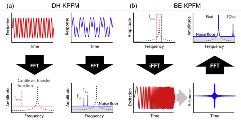
Scheme describing (a) Heterodyne KPFM and (b) Band Excitation KPFM
Specifications
- Sample up to buffer size
- Scan range (30x30 um, 80x80 um)
- Z height limit (<10 µm)
- Environmental Control
- Glove box (Ar filled)
- Environmental cells for gases: humidity, nonreactive
- Environmental cells for liquids: aqueous buffers, ionic liquids
- Temperature stage (sample heating 0-250 C)
- Interferometric Displacement Sensor (IDS) [Cypher AFM]
- High voltage source (100 V)
- Band Excitation Imaging and Spectroscopies
- FPGA Scanner Control
- PyAE workflows
- In-situ photoexcitation
Applications:
Electrical studies at the nanoscale using AFM has numerous applications in the field of electronics, including the characterization of nanoscale devices such as transistors, memory devices, and sensors. It can also be used to investigate the properties of materials used in electronic devices, such as thin films, coatings, and semiconductors.
Equipment:
Cypher AFM, MFP 3D AFM (Asylum Research) in ambient
Icon Dimension (Bruker) in ambient
Icon Dimension (Bruker) in Ar glovebox
Drive AFM (Nanosurf) in ambient
Contacts

Electronic and Dielectric Characterization

Electronic and Dielectric Characterization

Impedance spectroscopy

C-AFM