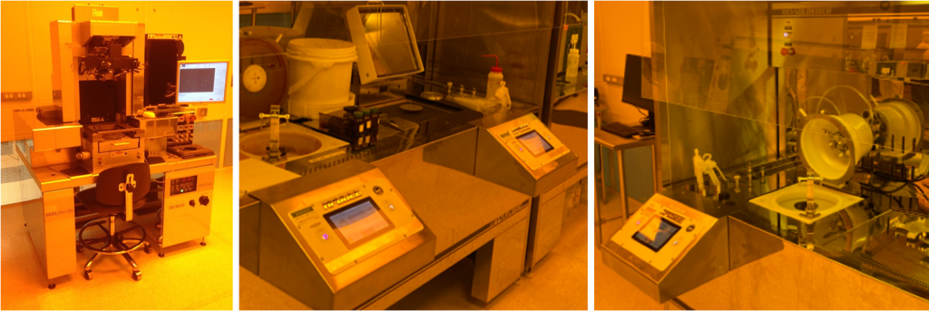
SUSS MicroTec MA6/BA6 Gen3 Contact Mask Aligner
Specifications
- Topside (TSA) and backside alignment (BSA) capabilities
- broadband (405-365nm) exposure optics
- Accuracy: <800nm, for TSA in vacuum contact mode, and 1mm for BSA
- 5x and 10x objectives
- Mask sizes 4”x 4” and 5” x 5”
- Allows patterning and alignment from 5mm x 5mm chip size up to 100mm wafer, with 10 mm thickness max
- Exposure modes:
- Vacuum contact, soft contact, hard contact, and proximity
- Constant power or constant dose
- Flood exposure, split exposure
CEE Apogee Spinners, Developer, and Bake Plates
Programmable spinner and bake combinations are critical for photoresist and electron beam resist reproducibility. Our spinner suite is capable of uniform coatings on full wafers down to chips. Our automated developer spinner offers better reproducibility in wafer development and minimizes chemical handling.
Specifications
- Spin speed: up to 12,000 rpm
- Spin speed acceleration: 0 to 23,000 rpm/s with a 200-mm substrate 0 to 3,000 rpm/s with a 6” × 6” × 0.250” photomask in a recessed chuck
- Spin speed repeatability: < 0.2 rpm
- Spin speed resolution: < 0.2 rpm
- Substrate sizes: < 1 cm to 200 mm round; 7” x 7” square
Recent Highlights
Strain tolerance of two-dimensional crystal growth on curved surfaces
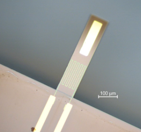
Real-Time Sensing of Single-Ligand Delivery with Nanoaperture-Integrated Microfluidic Devices

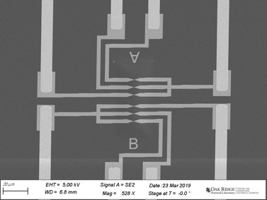
Photolithography pattern aligned with e-beam pattern.
Image credit: Jake Swett (Univ. of Oxford)

Microcantilevers with four-layer photolithography patterns aligned using SUSS MA6