Electron beam lithography (EBL) uses a focused beam of high energy electrons to chemically modify resists. The electron probe can be focused to much smaller areas than the diffraction limited optics in photolithography, which enables the highest resolution patterning into resist that the CNMS offers. Typically, the throughput for EBL is somewhat slower than photolithography, due to the need to raster the very small electron probe over the entire area to be patterned.
Applications
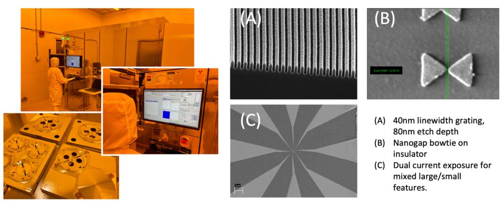
Optical metasurfaces and metasurface platforms, photonic crystals, optoelectronic and optical systems, plasmonic systems, nano-imprint lithography, field-effect transistors, and other features inaccessible to optical lithography.
Specifications
• Low and High Current Write modes available (100pA – 100nA)
• Dual Current Writing For High Throughput Processing of samples combinations of small and large features
• Integrated optical microscope for facile sample alignment of pieces with partial marks
• 125Mhz Scan Speed (2.5x Faster than before)
• 0.5nm step size
• Nominal spot size approaching 4nm
• Field sizes up to 1mm can be written without stage movement
• Less than 9nm Stitching and Overlay Accuracy
• Layout BEAMER© is used for file conversion and proximity correction.
Recent Highlights
Topological nanostructures enable nonlinear light generation