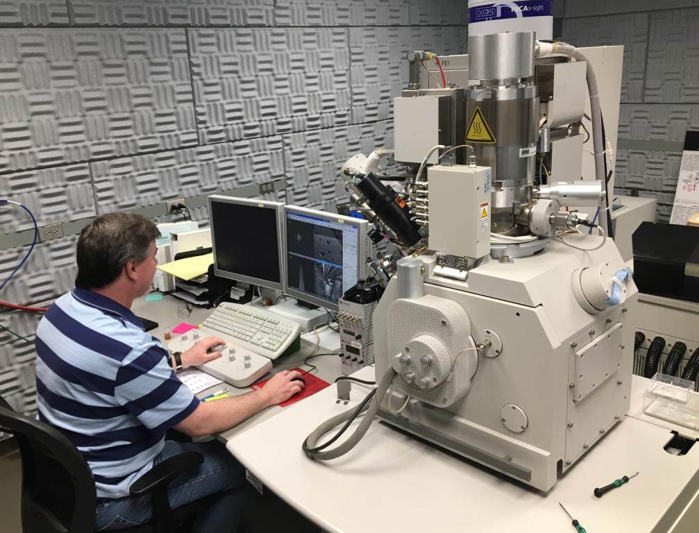
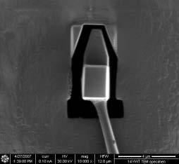
The FEI Nova 200 Dual Beam SEM/FIB is used to prepare ~100 nm needle shaped specimens and <100 nm lamella for atom probe tomography (APT) and transmission electron microscopy (TEM) experiments.
The electron and ion beams are focused onto an eucentric stage position at a 52° angle allowing for simultaneous milling and imaging using the ion and electron beams, respectively. The nanoscale ion beam allows for high precision sample fabrication at 30 kV, while lower voltage beams are used to remove ion beam damaged regions from the sample surfaces.
A Kleindiek nanomanipulator can be used to liftout and/or electrically bias site-specific regions of interest. The microscope is equipped with Continuous Dynode Electron Multiplier (CDEM), Everhart-Thronly (ET), in-lens (TLD), and Scanning Transmission Electron Microscope (STEM) electron and ion detectors as well as an EDAX octane elect X-ray detector for energy dispersive X-ray diffraction (EDS) measurements.
Specifications
Sidewinder FIB Column
- Liquid metal Ga+ ion source
- Resolution: 5 nm
- 50x minimum magnifications at 5 kV
- 1 to 30 kV accelerating voltage
- 1.5 pA to 20 nA accelerating voltage
SEM Column
- 0.9 nm resolution at 15 kV
- 20 nA maximum beam current
- CDEM, ET, TLD, and STEM detectors
EDAX Octane Elect X-Ray Detector