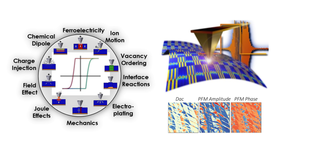
Piezoresponse Force Microscopy is used to detect mechanical responses of an AFM tip used as a top electrode when an electric signal is applied to it to excite the sample. Despite the primary response is obtained from piezo and ferroelectric materials via the inverse piezoelectric effect, this technique can been applied to study a wider range of nanoscale electromechanical phenomena, such as ionic motion or defects ordering in crystalline materials.
Features
Available modes:
- Piezoresponse force microscopy (PFM) measures the local electromechanical deformation in response to an AC voltage applied through the tip. The strength of the piezoresponse and the polarity of the polarization can be extracted from the amplitude and phase signals, respectively.
- Switching spectroscopy PFM (SS-PFM), a DC voltage is applied typically to induce polarization switching in ferroelectric materials while the piezoresponse during and between DC triangle square pulses is measured and recorded. PFM hysteresis loops can be measured using SSPFM.
- Contact Kelvin probe microscopy (cKPFM) is similar to SSPFM with the difference that over multiple cycles a varying DC read voltage is applied between the write pulses that are applied to change the polarization. This approach helps to distinguish between real ferroelectric switching and electrostatic artifacts.
- Quantitative PFM utilizes electrostatic blind spots along the cantilever mode shape, or intrinsically calibrated measurement of tip displacement utilizing interferometric detection. These modes are less prone to electrostatic influences, leading to more reliable investigations of ferroelectricity and allow quantification off effective piezoelectric coefficients on the nanoscale
- Thermal PFM (ThPFM) enables to measure electromechanical properties under local heating conditions induced by laser thermal control of the tip.
Specifications
- Sample up to buffer size
- Scan range (30x30 um, 80x80 um)
- Z height limit (<10 µm)
- Environmental Control
- Glove box (Ar filled)
- Environmental cells for gases: humidity, nonreactive
- Temperature stage (sample heating 0-250 C)
- Interferometric Displacement Sensor (IDS) [Cypher AFM]
- High voltage source (100 V)
- Band Excitation Imaging and Spectroscopies
- FPGA Scanner Control
- PyAE workflows
- In-situ photoexcitation
Applications
- Ferroelectric and multiferroic materials
- Batteries
- Ionic conductors
- 2D heterostructures
Equipment
- Cypher AFM, MFP 3D AFM (Asylum Research) in ambient
- Icon Dimension (Bruker) in ambient
- Icon Dimension (Bruker) in Ar glovebox
- Drive AFM (Nanosurf) in ambient
- Variable temperature UHV Omicron AFM
Contacts

Correlative PFM modes

Correlative PFM & SMIM, cKPFM, 2D and van der Waals ferroelectrics

Wurzite and hexagonal ferroelectrics, phase transitions
.

Quantitative PFM

Nanoscale Electromechanics, ferroelectric surfaces and ferroic domain walls

Advanced electromechanical spectroscopies