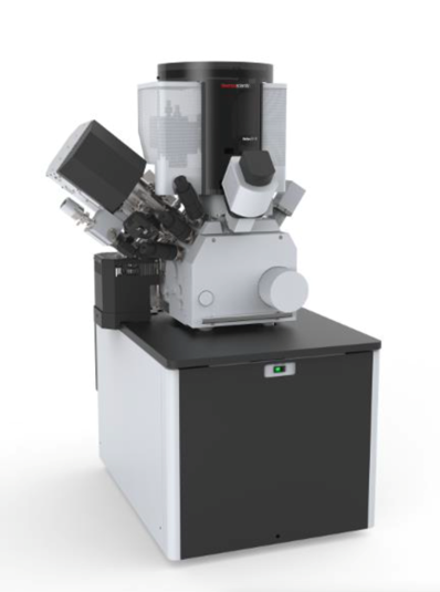
The Helios Hydra cryogenic plasma focused ion beam (cryo-PFIB) allows users and scientists to site-specifically mill into materials to reveal buried structures and interfaces and characterize surfaces and buried features down to the nanoscale.
The plasma beam enables rapid milling, allowing larger volumes to be milled than a conventional Ga+ FIB beam. Cryogenic sample temperatures and four plasma beam ion sources (Xe, Ar, O, N) provide versatility for working with a wide variety of materials, from hard materials such as oxides to soft frozen-hydrated biological materials and complex composite systems like solid-liquid interfaces.
A high-resolution, low-voltage scanning electron microscope (SEM) beam combined with secondary electron (SE) and backscatter electron (BSE) detectors allows structural characterization with topographical and compositional contrast down to the nanometer scale and the ability to image beam-sensitive materials.
A large solid-angle energy-dispersive X-ray spectrometer (EDS) and electron backscatter detector (EBSD) additionally allow compositional and atomic lattice properties to be characterized at the nanoscale, while automated milling and characterization allow three-dimensional (3D) analysis.
A cryogenic “lift-out” system further enables preparation of electron-transparent cross-sectional cryogenic transmission electron microscopy (cryo-TEM) samples extracted from larger samples.
Specifications
SEM Column
- 350 eV to 30 keV beam energies
- Beam currents 0.8 pA to 100 nA
- Sub-nm resolution from 2 to 15 keV, nm-scale resolution down to 350 eV with beam deceleration
PFIB Column
- 500 eV to 30 keV beam energies
- Beam currents 1 pA to 2.5 µA at 30 keV
- More than 20nm resolution at 30 keV (Xe ions)
- Xe, Ar, O, and N ion sources, with more than 10 minutes switching time
- Large area milling (100’s of µm)
Detectors
- Secondary electron (SE) – conventional and through-the-lens detectors (TLD)
- Backscatter electron (BSE) TLD
- Ion-conversion and electron (ICE) detector for secondary ions (SIs) and SEs
- Large solid-angle energy-dispersive X-ray spectrometer (EDS)
- Electron backscatter detector (EBSD)
Cryogenic system
- Cryogenic sample preparation (plunge freezing, metal sputtering, freeze fracturing) and vacuum transfer
- Sample temperatures down to ~ 90 K
- Cryogenic “lift-out” for cryogenic transmission electron microscopy (cryo-TEM) sample preparation