Two Plasma Atomic Layer Deposition Systems (ALD) allows deposition of highly conformal thin films on virtually any topography at relatively low temperatures. Plasma ALD allows for precise deposition of ultra-thin and pinhole free films from a single atomic layer up to several nanometers. The two defining characteristics of ALD are self-limiting layer by layer growth and highly conformal coating of extreme high aspect ratio topography. The addition of plasma capability allows for ALD processing temperatures as low as 30oC. Passivation and/or functionalization of high aspect ratio features, ultra-thin gate dielectrics, reduction of pore size in porous materials, conformal coating of nanoparticles, nanowires, posts, cavities, trenches, etc. Some films make excellent etch masks. Low temperature deposition on polymer substrates.
Specifications/Capabilities
- Deposition of highly conformal, ultra-thin and pinhole free films
- Single 4” wafer or small chip processing
- Plasma or Thermal ALD
- Inductively Coupled Plasma RF power up to 600 watts
- Deposition temperatures from 30°C to 400°C
ALD Materials Available
- Aluminum Oxide
- Aluminum Nitride
- Hafnium Oxide
- Hafnium Nitride
- Vanadium Oxide
- Silicon Oxide
- Titanium Oxide
Applications
Passivation and/or functionalization of high aspect ratio features, ultra-thin gate dielectrics, reduction of pore size in porous materials, conformal coating of nanoparticles, nanowires, posts, cavities, trenches, etc. Some films make excellent etch masks. Low temperature deposition on polymer substrates.
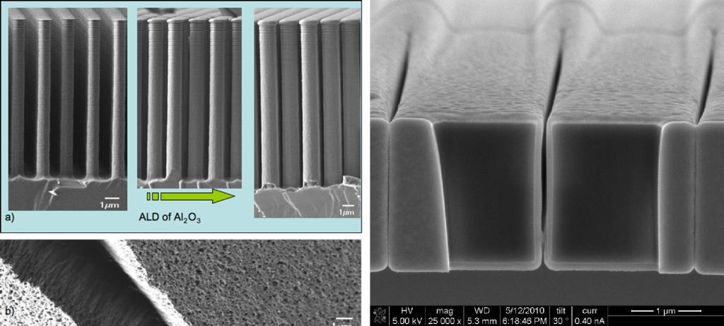
Left: Transformation of photolithographically patterned pillar arrays in high aspect ratio nanogap array for studies of transport and reactivity under nanoscale confinement. Right: Nanogap reduction of Electron Beam lithography patterned features via conformal coating of ALD aluminum oxide.
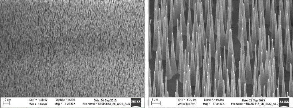
Functionalization of RIE black silicon nanopillar arrays with 2nm of conformal ALD Hafnium oxide coating.
Specifications
- Deposition of highly conformal, ultra-thin and pinhole free films
- Single 4” wafer or small chip processing
- 4” cross wafer uniformity typically < +/-1%
- Plasma or Thermal ALD
- Inductively Coupled Plasma RF power up to 600 watts
- Deposition temperatures from 30 °C to 400 °C
Recent Highlights