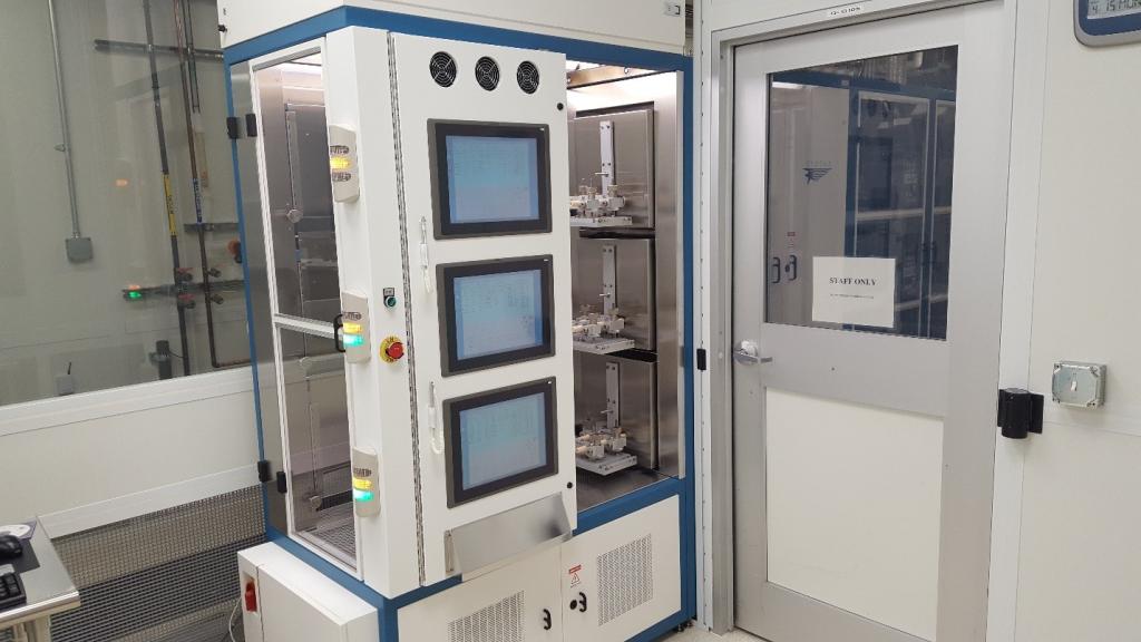
The Tystar Furnace is used to grow or deposit a variety of thin films on silicon or quartz substrates. It is a batch process, three tube high temperature horizontal furnace stack. The “stack” consists of three independent systems or tubes that can each process up to 50 wafers per run. It is capable of processing samples up to 8” in diameter. Substrate materials used here are typically limited to clean silicon or quartz.
Tube 1 is an atmospheric pressure system dedicated to growing high purity thermal Silicon dioxide (SiO2) thin films on silicon substrates. It is capable of processing temperatures up to 1150 °C.
Tube 2 is a low pressure chemical vapor deposition (LPCVD) system configured to deposit various high quality silicon nitride thin films. It is capable of processing temperatures up to 900 °C. This tool can deposit stoichiometric silicon nitride (Si3N4) or low stress non-stoichiometric silicon nitride. Film stress and/or stoichiometry can be tuned for specific applications.
Tube 3 is a low pressure chemical vapor deposition (LPCVD) system configured to deposit various oxides and silicon thin films. It is capable of processing temperatures up to 700 °C. This tool can deposit intrinsic poly-silicon, doped poly-silicon (N-Type), amorphous silicon, low temperature silicon oxide (LTO), and doped oxides such as borophosphosilicate glass (BPSG) and phosphosilicate glass (PSG).
Applications
- Silicon dioxide as an electrical insulator, gate dielectric, MEMS device material, sacrificial etch layer, etch hard mask.
- Silicon nitride as a passivation layer, free standing cantilevers and membranes.
- Poly-silicon as a MEMS device material, doped as the active layer in a thin film transistor, In-situ bimodal deposition of LTO/silicon metamaterial films.
Specifications
- 4” or 6” wafer size
- Up to 50 wafer batch processing
- Growth/deposition temperatures range from 400 °C to 1150 °C
- Cross wafer thickness uniformity typically < +/- 3%
Recent Publications
Realization of an all-dielectric zero-index optical metamaterial