Project Details
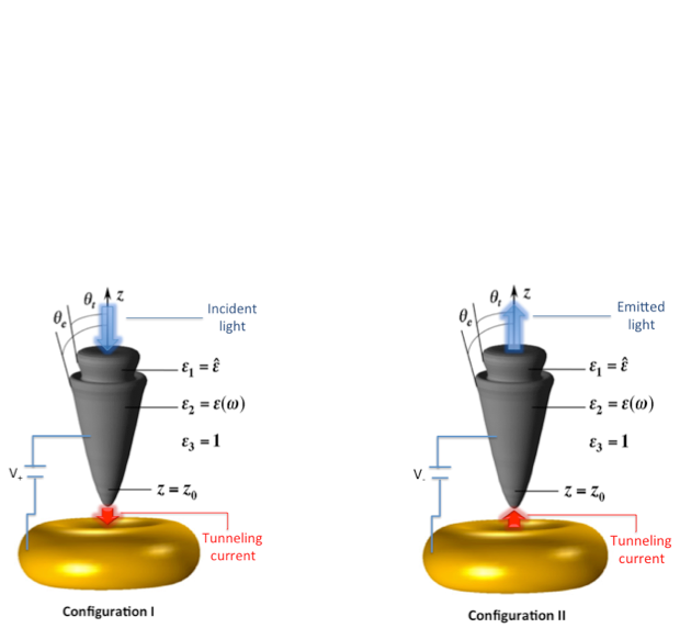
Dynamic imaging of nanoscale processes is crucial for many applications in physics, chemistry and biology. Imaging techniques such as the scanning electron microscopy (SEM) provide an excellent spatial resolution but utilize a sophisticated beam focusing setup and are not designed to resolve temporal dynamics. On the other hand, for applications that do not require sub-nanometer resolution, electron point projection microscopy (ePPM) provides a viable alternative to SEM. An attractive feature of ePPM is that electron emission can be timed optically by applying a pico- or femto- second laser pulse to a metallic nanotip. This furnishes ePPM with a unique capability to simultaneously deliver spatial and temporal resolution. However, to permit pulse delivery and reduce unwanted sample illumination and spurious scattering by the laser field, the nanotip must be positioned far above (several micrometers) the surface of a sample. This, in turn, limits the spatial resolution of ePPM. To circumvent this shortcoming, we are investigating a new type of nanotip electron source in the form of a metalized dialectic tip. The electron emission is realized by a pulsed optical excitation of surface plasmons in the metallic medium and their subsequent decay accompanied by electron tunneling from the nanotip. The optical pulse is delivered inside of the optically short dielectric structure that constitutes the core of the nanotip, which enables one to bring the electron source arbitrarily close to the surface of a sample and, therefore, significantly increase the spatial resolution of ePPM.

