
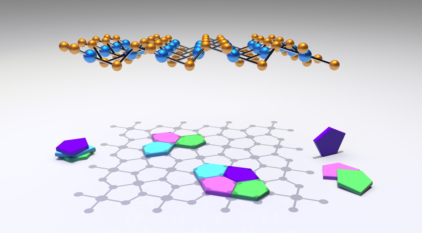
November 2, 2017 – A semiconducting material with a puckered pentagonal atomic structure, characterized by Oak Ridge National Laboratory, could rival graphene and black phosphorus as a viable option for nanoscale electronics. The ORNL-led team studied a novel two-dimensional, or atomic-thin, layered material called palladium diselenide, or PdSe2. The team unveiled that the atoms of the material chemically bond in five-sided structures. This causes the resulting layers to “pucker” and makes the material exhibit properties that could benefit future optoelectronics. “The band gap of the material changed significantly as we exfoliated layers of PdSe2 from a bulk crystal,” ORNL’s Kai Xiao said. “The ability to tune the material’s band gap from zero in the bulk to approximately 1.3 electron volts in the monolayer opens exciting new options for nanoelectronics.” The team published their work in the Journal of the American Chemical Society and plans to grow scalable, large-area 2D PdSe2 crystals.


