-
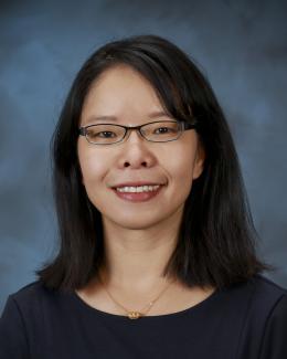
ORNL researcher Miaofang Chi refines her microscopy techniques toward understanding how and why materials have certain properties.
-
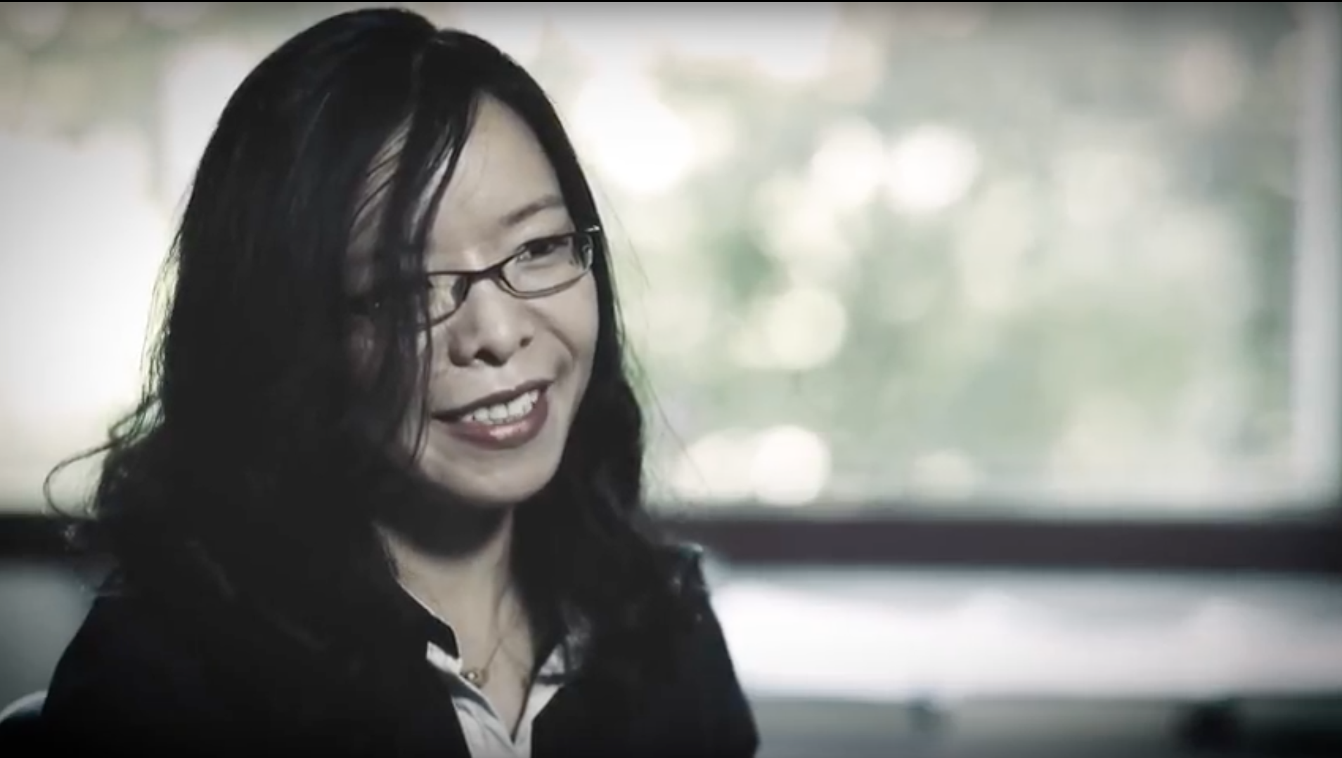
ORNL researcher Miaofang Chi refines her microscopy techniques toward understanding how and why materials have certain properties.


-
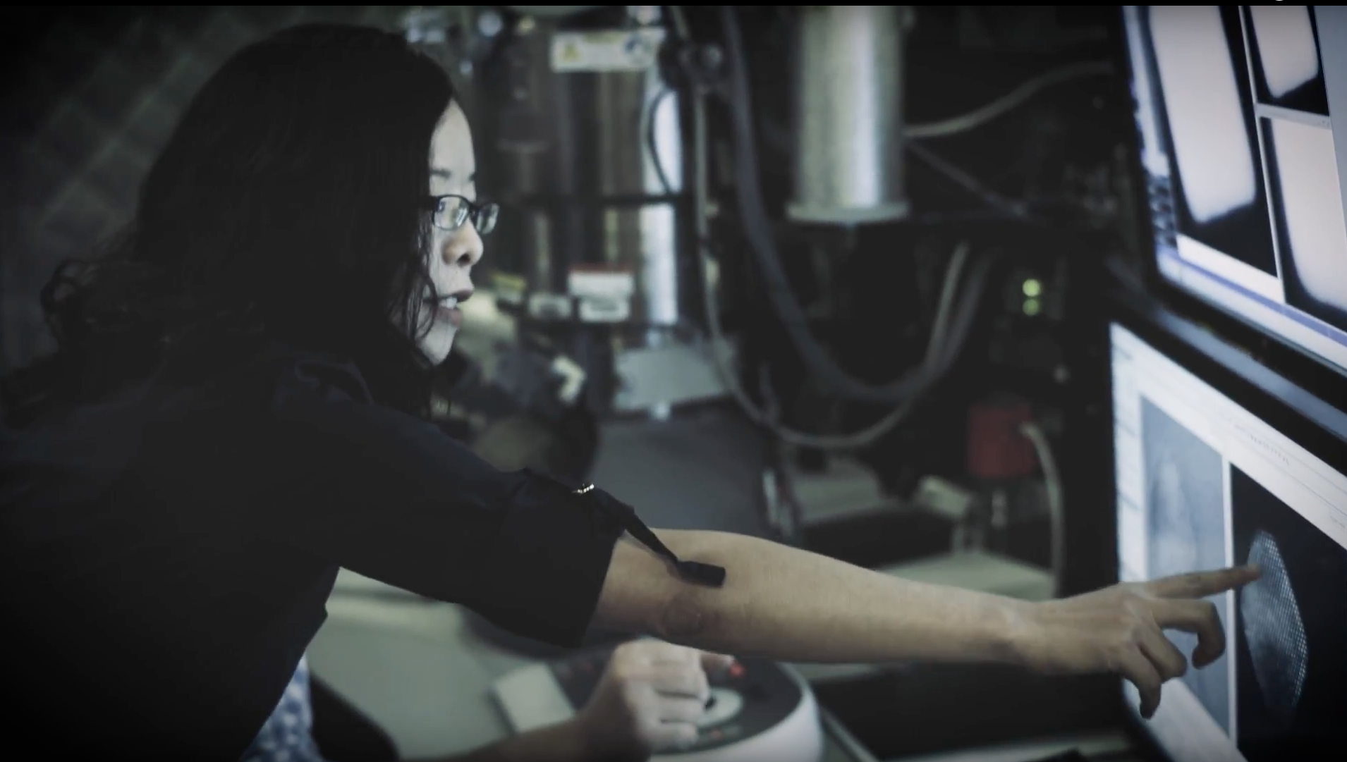
ORNL researcher Miaofang Chi refines her microscopy techniques toward understanding how and why materials have certain properties.
-
ORNL researcher Miaofang Chi refines her microscopy techniques toward understanding how and why materials have certain properties.
Microscopist develops new techniques for observing how materials function
January 8, 2018 – Material surfaces and interfaces may appear flat and void of texture to the naked eye, but a view from the nanoscale reveals an intricate tapestry of atomic patterns that control the reactions between the material and its environment. Electron microscopy allows researchers to probe these hidden configurations by using a powerful electron beam to illuminate a subject with far greater magnification and resolution than light microscopy.
Miaofang Chi gained expertise in using these microscopes during her early studies to become a materials scientist. Though they were not as advanced as today’s models, the microscopes tapped into her interest in photography and allowed her to image a material’s “nanoscopic artwork.”
“I felt like electron microscopy opened up an entirely different world for me,” Chi said. “You simply never imagined that one could actually arrange the atoms in as pretty a pattern as nature does.”
Now, as a research staff member at the Department of Energy’s Oak Ridge National Laboratory, Chi develops novel electron microscopy techniques to help scientists solve problems and synthesize materials with optimal physical properties.
Computer simulations can reliably predict the arrangement of atoms in the bulk of a material, but often have difficulty modeling the asymmetric interfaces and boundaries. Chi studies how these interfacial configurations and chemistries control materials properties and introduce limitations to the performance of energy storage and transport materials.
As a researcher in the Electron & Atom Probe Microscopy group at ORNL's Center for Nanophase Materials Sciences, Chi has advanced in situ microscopy techniques that now enable researchers to watch interfaces form and evolve at the atomic level by introducing different sample environments, such as elevated or cryo temperatures, liquids or gases. These conditions can mimic the operating conditions of a real device, such as the electrochemical cycling in batteries or solid oxide fuel cells.
“Advanced atomic-scale electron microscopy provides great insights that help us to understand how materials function and the roles of each atom,” she said.
In addition to the significant technical resources available for research, the greatest benefit of working at the national labs is the plethora of readily available scientific expertise. All it takes to access this diverse well of knowledge, Chi said, is to leave your office and talk to someone new.
“It’s easy to walk next door or to the next building to find any answer that you are looking for,” she said. “In particular, discussing your ideas with experts across different disciplines can be extremely inspiring. Learning how they take different approaches to solve problems can often stimulate new ideas and solutions for my own research. What I love the most about my work at ORNL is that I get to work together with many scientists, all having different expertise across many scientific fields. The friendly and collaborative working environment has significantly benefited my career.”
Chi likes to broaden her knowledge in research fields beyond materials science, as the CNMS Electron & Atom Probe Microscopy group lies at the nexus of theory, observation and nanofabrication research at the lab.
“We link materials structure, chemistry and function together,” she said. “Microscopy can presently be used to “see” atoms routinely; thus, our current efforts in creating novel microscopy techniques are specifically aimed at directly probing the functionality of materials with atomic or molecular resolution, at desired rapid time scales, and under real operation or formation environments. Such capability will enable the design of new functional materials and interfaces.
“This is the future of microscopy,” Chi said.
As the bridge between so many materials fields of study, Chi is also able to reach out to other scientists to demonstrate how ORNL’s advanced microscopy capabilities can accelerate the discovery and innovation process.
“Many times materials scientists do not know there are microscopy techniques on the horizon that may enable new discoveries,” Chi said. “What I’m really interested in is to advance these emerging techniques and to tailor and optimize them to address scientific questions in the material science field.”
Chi estimates the optimal work balance is usually five days of analysis for every one day of hands-on microscopy. This ratio gives her plenty of time to design the experiments, analyze the data, confer with other scientists, and discuss how to interpret certain physical properties of a material, which often leads to her going back to the microscope to corroborate the phenomena at a different length scale.
“To maintain this balance, though, a researcher must do their homework ahead of time,” Chi said. Properly preparing for an experiment and doing the background research is a vital first step in any process, and is key to obtaining the best results and to avoid wasting valuable time and effort.
“It’s always important to do as much research as possible before you put a sample in the microscope and set up an experiment—if you don’t take the necessary time prior to execution, you can easily overlook or misinterpret the features you’re seeing,” she said.
Of all the lessons Chi has learned since joining ORNL, the most valuable ones are those that taught her how to create a plan and follow it through until the end.
“When you are a student, you don’t have to think about initiating a project,” she said. “As an independent scientist, you must learn to look at everything strategically. Evaluate five or ten years into the future and see what this particular project can lead to, and will it be interesting to the scientific community, and importantly, will it be interesting to yourself.”
The Center for Nanophase Materials Sciences is a DOE Office of Science User Facility. ORNL is managed by UT-Battelle for the Department of Energy's Office of Science, the single largest supporter of basic research in the physical sciences in the United States. DOE’s Office of Science is working to address some of the most pressing challenges of our time. For more information, please visit http://energy.gov/science/. – By Sean Simoneau