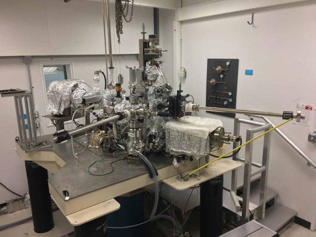
This low temperature high magnetic field scanning tunneling microscope (LTHB STM) and molecular-beam-epitaxy (MBE) combined system enables structural, electronic, and spin studies of the surfaces of quantum materials. The MBE chamber provides the capability of in situ construction of films or cleaving or sputtering and annealing to restore the surface of ex situ transferred samples. The STM can map the conductivity, work function and spin configuration of related quantum phenomenon with atomic scale precision at extremely low temperatures and high magnetic fields.
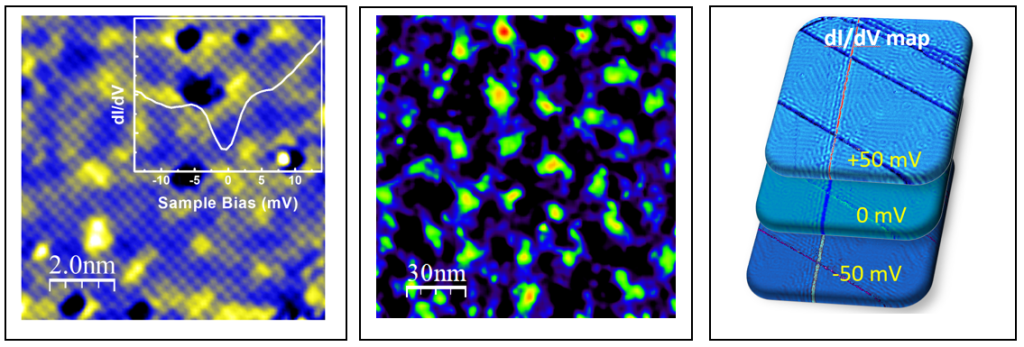
a): Atomic resolution and average dI/dV spectroscopy of Iron based superconductor Ba(FeCo)2As2. b) Vortex structure of Ba(FeCo)2As2 under 6 Tesla. c) dI/dV mapping of Au(111) at various sample bias. All data were taken at 4.2 K.
Science Overview
The CNMS LTHB-MBE STM system consists of three ultra-high vacuum (UHV) chambers which are connected for sample transfer without external exposure. This unique feature provides the ability to characterize newly grown or cleaved materials in a carefully controlled environment without surface contamination.
The first chamber is a sample preparation chamber and MBE chamber. Routine surface science techniques like Argon sputtering, electron bombardment heating or direct heating are equipped to clean samples or substrates in vacuum. High quality thin films can be grown by MBE on substrate at variable temperatures. Three MBE sources include one K-cell evaporator and two electron beam bombardment evaporators. Low energy electron diffraction (LEED) is available to verify the surface crystallinity of the films.
The second chamber is equipped with a low temperature cleaving stage for in situ cleavage of single crystal samples. It also serves as a chamber for specific growth (two evaporator sources) on substrates maintained on cryogenic temperature.
The third chamber is the STM chamber, for atomically resolved images and spectroscopy. This STM is suitable for extended dI/dV spectroscopy mapping with atomic precision up to days. Spin-polarized STM/S with a Cr/Ni coated tungsten tip has been developed for resolving the spin structure of quantum materials. The microscope can operate from 2.0 K up to room temperature with 9 Tesla magnetic field capability and energy resolution lower than 0.7 meV.
Applications
More detailed examples can be found in the following papers: Nano Letters 17, 1642 (2017); Scientific Reports 7, 949 (2017).
Specifications
General
- Samples must be UHV compatible, able to be mounted on a metal transfer plate and relatively flat
- Samples must be conductive
- Sample size:
- Type I: Length ~ 3-4 mm, width ~3-4 mm, thickness: up to 1.5 mm
- Type II: Length ~ 10 mm, width ~1-2 mm, thickness: up to 0.5 mm
- Inserted sample can be prepared by in-situ cleaving, Ar+ sputtering or heated in UHV vacuum
- Cleavage stage temperature: 10 K ~ 300 K
Growth
- Sample stage temperature: 20 ~1500 K
- One K-cell evaporator
- Two electron beam bombardment evaporators
STM
- Scanner range: XY: 2 µm/0.6 µm, Z: 0.3 µm/0.08 µm (77 K/4.2 K)
- Coarse motion of X or Y stage: ±0.5 mm
- Temperature: 2.0 ~ 300 K
- Magnetic field: vertical direction up to 9 Tesla
- Energy resolution: < 0.7 meV
- Note that specific positioning of the STM tip on the sample is not possible.