Scanning Tunneling Microscopy
The STM group's mission is to "To understand and control the correlations of atomic structure with electronic, magnetic, and transport properties in quantum materials through the development of scanning tunneling microscopy methods.”
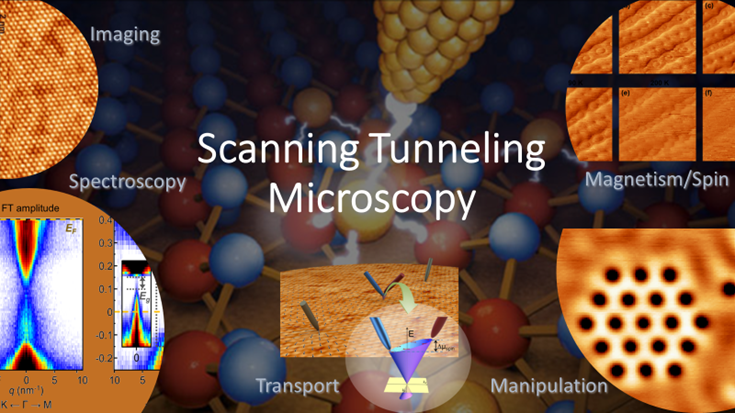
The Scanning Tunneling Microscopy (STM) Group at the Center for Nanophase Materials Sciences (CNMS) specializes in atomic resolution imaging, electronic density of states mapping, nanoscale electron transport survey, and atom and molecule manipulation through the development and utilization of STM techniques.
Research is focused on establishing correlation of physical properties with atomic structures and controlling material processes at an atomic scale to tailor electronic wavefunctions and interactions. Unique capabilities include the only dilution refrigeration vector magnet STM in a user facility, the only spin-polarized 4-probe STM in the world, and a new scanning NV microscope. These cover a wide range of sample environments, including temperatures of 40 mK to 300K, magnetic fields up to 9 T, and ultra-high vacuum.
The STM systems are integrated with material growth capabilities by molecular beam epitaxy (MBE), pulse laser deposition (PLD), and substrate-assisted on-surface chemical reactions. Samples can be shared between microscopes via vacuum suitcases. These capabilities have enabled the first identification of skyrmions in a van der Waals magnet; the first direct evidence of spin-momentum locking in topological materials through the spin chemical potential; the first direct observation of single-vacancy based non-volatile resistive switching (NVRS); and the first demonstration of single molecule telegraphy across a surface.