
Stacking layers of nanometer-thin semiconducting materials at different angles is a new approach to designing the next generation of energy-efficient transistors and solar cells. The atoms in each layer are arranged in hexagonal arrays.

To tailor tiny nanocrystals for catalysts, semiconductors and other applications, scientists must predict what happens inside the particle, at the boundary and in the solvent during particle growth.
")
Understanding where and how phase transitions occur is critical to developing new generations of the materials used in high-performance batteries, sensors, energy-harvesting devices, medical diagnostic equipment and other applications.
A new era of electronics and even quantum devices could be ushered in with the fabrication of a virtually perfect single layer of “white graphene,” according to researchers at the Department of Energy’s Oak Ridge National Laboratory.

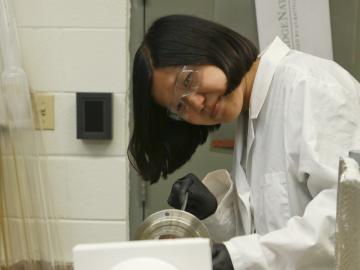
Miaofang Chi of the Center for Nanophase Materials Sciences at the Department of Energy's Oak Ridge National Laboratory has earned the ORNL Director’s Award for Outstanding Individual Accomplishment in Science and Technology.
Four researchers from the Department of Energy's Oak Ridge National Laboratory have been elected fellows of the American Physical Society (APS), one of the nation's top professional organizations for scientists.
Jaime Fernandez-Baca, Sergei Kalinin, Mark

Electron microscopy researchers at the Department of Energy’s Oak Ridge National Laboratory have developed a unique way to build 3-D structures with finely controlled shapes as small as one to two billionths of a meter.
Quasiparticles—excitations that behave collectively like particles—are central to energy applications but can be difficult to detect.
Steady progress in the development of advanced materials has led to modern civilization’s foundational technologies—better batteries, resilient building materials and atom-scale semiconductors.