

Oak Ridge National Laboratory researchers serendipitously discovered when they automated the beam of an electron microscope to precisely drill holes in the atomically thin lattice of graphene, the drilled holes closed up.
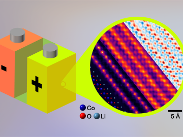
Oak Ridge National Laboratory researchers demonstrated an electron microscopy technique for imaging lithium in energy storage materials, such as lithium ion batteries, at the atomic scale.
To advance sensor technologies, Oak Ridge National Laboratory researchers studied piezoelectric materials, which convert mechanical stress into electrical energy, to see how they could handle bombardment with energetic neutrons.
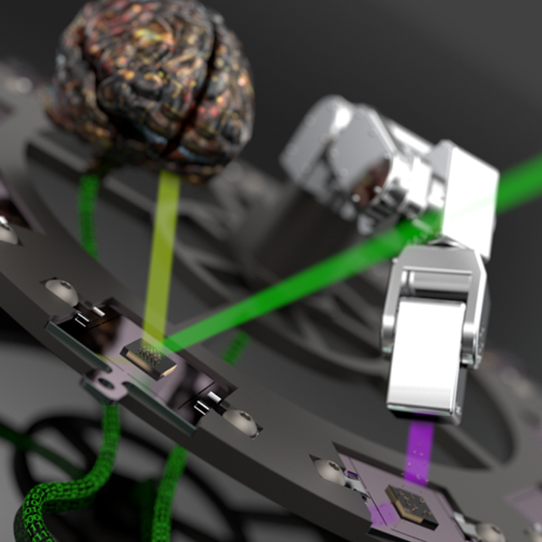
Combining expertise in physics, applied math and computing, Oak Ridge National Laboratory scientists are expanding the possibilities for simulating electromagnetic fields that underpin phenomena in materials design and telecommunications.
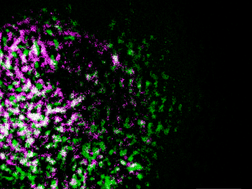
Oak Ridge National Laboratory researchers have built a novel microscope that provides a “chemical lens” for viewing biological systems including cell membranes and biofilms.
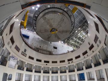
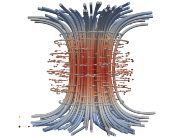
ITER, the world’s largest international scientific collaboration, is beginning assembly of the fusion reactor tokamak that will include 12 different essential hardware systems provided by US ITER, which is managed by Oak Ridge National Laboratory.

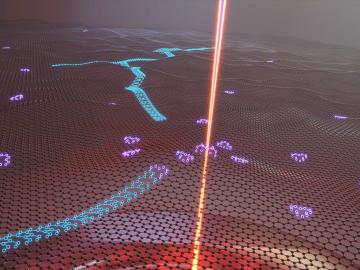
Scientists at Oak Ridge National Laboratory used a focused beam of electrons to stitch platinum-silicon molecules into graphene, marking the first deliberate insertion of artificial molecules into a graphene host matrix.
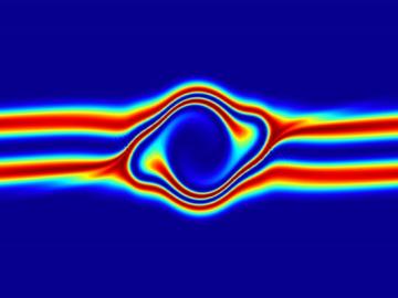
The prospect of simulating a fusion plasma is a step closer to reality thanks to a new computational tool developed by scientists in fusion physics, computer science and mathematics at ORNL.