![White car (Porsche Taycan) with the hood popped is inside the building with an american flag on the wall.](/sites/default/files/styles/featured_square_large/public/2024-06/2024-P09317.jpg?h=8f9cfe54&itok=m6sQhZRq)
Filter News
Area of Research
- (-) Materials (82)
- (-) Neutron Science (27)
- Advanced Manufacturing (10)
- Biology and Environment (25)
- Clean Energy (64)
- Computer Science (1)
- Energy Frontier Research Centers (1)
- Fusion and Fission (8)
- Isotope Development and Production (1)
- Isotopes (2)
- Materials Characterization (1)
- Materials for Computing (13)
- Materials Under Extremes (1)
- National Security (8)
- Nuclear Science and Technology (6)
- Quantum information Science (1)
- Supercomputing (34)
News Type
News Topics
- (-) 3-D Printing/Advanced Manufacturing (21)
- (-) Big Data (3)
- (-) Materials Science (60)
- (-) Nanotechnology (31)
- (-) Polymers (11)
- Advanced Reactors (2)
- Artificial Intelligence (10)
- Bioenergy (13)
- Biology (9)
- Biomedical (13)
- Biotechnology (1)
- Buildings (3)
- Chemical Sciences (27)
- Clean Water (3)
- Climate Change (5)
- Composites (5)
- Computer Science (23)
- Coronavirus (10)
- Critical Materials (8)
- Cybersecurity (5)
- Decarbonization (7)
- Energy Storage (27)
- Environment (18)
- Exascale Computing (2)
- Fossil Energy (1)
- Frontier (3)
- Fusion (5)
- Grid (4)
- High-Performance Computing (5)
- Isotopes (11)
- ITER (1)
- Machine Learning (6)
- Materials (62)
- Mathematics (1)
- Microscopy (18)
- Molten Salt (2)
- National Security (4)
- Net Zero (1)
- Neutron Science (78)
- Nuclear Energy (12)
- Partnerships (11)
- Physics (27)
- Quantum Computing (3)
- Quantum Science (12)
- Renewable Energy (1)
- Security (3)
- Space Exploration (3)
- Summit (6)
- Sustainable Energy (10)
- Transformational Challenge Reactor (3)
- Transportation (11)
Media Contacts
![Gobet_Advincula Portrait](/sites/default/files/styles/list_page_thumbnail/public/2020-02/2020-P00191.png?h=8f9cfe54&itok=MA0hIqj6)
Rigoberto “Gobet” Advincula has been named Governor’s Chair of Advanced and Nanostructured Materials at Oak Ridge National Laboratory and the University of Tennessee.
![Scanning probe microscopes use an atom-sharp tip—only a few nanometers thick—to image materials on a nanometer length scale. The probe tip, invisible to the eye, is attached to a cantilever (pictured) that moves across material surfaces like the tone arm on a record player. Credit: Genevieve Martin/Oak Ridge National Laboratory; U.S. Dept. of Energy.](/sites/default/files/styles/list_page_thumbnail/public/2020-01/2019-P15115.jpg?h=c6980913&itok=o69jyoNw)
Liam Collins was drawn to study physics to understand “hidden things” and honed his expertise in microscopy so that he could bring them to light.
![ORNL-developed cryogenic memory cell circuit designs fabricated onto these small chips by SeeQC, a superconducting technology company, successfully demonstrated read, write and reset memory functions. Credit: Carlos Jones/Oak Ridge National Laboratory, U.S. Dept. of Energy](/sites/default/files/styles/list_page_thumbnail/public/2020-01/2019-P17636.png?h=39b94f55&itok=udTwXJwT)
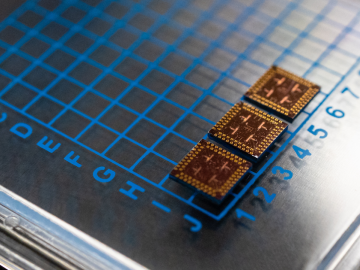
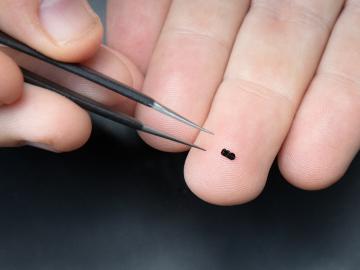
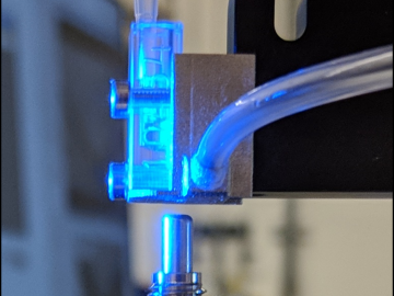
Scientists at have experimentally demonstrated a novel cryogenic, or low temperature, memory cell circuit design based on coupled arrays of Josephson junctions, a technology that may be faster and more energy efficient than existing memory devices.
![The students analyzed diatom images like this one to compare wild and genetically modified strains of these organisms. Credit: Alison Pawlicki/Oak Ridge National Laboratory, US Department of Energy.](/sites/default/files/styles/list_page_thumbnail/public/2019-11/RI4362007.png?h=37702503&itok=9lQReLRe)
Students often participate in internships and receive formal training in their chosen career fields during college, but some pursue professional development opportunities even earlier.
![SNS researchers](/sites/default/files/styles/list_page_thumbnail/public/2019-11/2019-P15103_1.jpg?h=c6980913&itok=OoO429Iv)
Scientists at the U.S. Department of Energy’s Brookhaven National Laboratory have new experimental evidence and a predictive theory that solves a long-standing materials science mystery: why certain crystalline materials shrink when heated.
![CellSight allows for rapid mass spectrometry of individual cells. Credit: John Cahill, Oak Ridge National Laboratory/U.S. Dept of Energy](/sites/default/files/styles/list_page_thumbnail/public/2019-10/4CellSightPhoto_0.png?h=67debf3e&itok=fmsxiN_b)
Researchers at the Department of Energy’s Oak Ridge National Laboratory have received five 2019 R&D 100 Awards, increasing the lab’s total to 221 since the award’s inception in 1963.
![Representatives from The University of Toledo and the U.S. Department of Energy’s Oak Ridge National Laboratory (ORNL) in Tennessee are teaming up to conduct collaborative automotive materials research.” Credit: University of Toledo](/sites/default/files/styles/list_page_thumbnail/public/2019-10/Oak%20Ridge%20Nat%20Lab%20group%20photo_0.jpeg?h=1e7f2295&itok=pITK15-V)
ORNL and The University of Toledo have entered into a memorandum of understanding for collaborative research.
![low-cost material can be used as an additive to increase thermal insulation performance](/sites/default/files/styles/list_page_thumbnail/public/2019-09/2019-P09265_0.jpg?h=036a71b7&itok=tVT2cC3V)
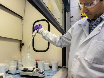
Quanex Building Products has signed a non-exclusive agreement to license a method to produce insulating material from ORNL. The low-cost material can be used as an additive to increase thermal insulation performance and improve energy efficiency when applied to a variety of building products.
![The core of a wind turbine blade by XZERES Corporation was produced at the MDF using Cincinnati Incorporated equipment for large-scale 3D printing with foam.](/sites/default/files/styles/list_page_thumbnail/public/2019-06/image%201_2019-P01384_0.jpg?h=036a71b7&itok=ohbWG8Xd)
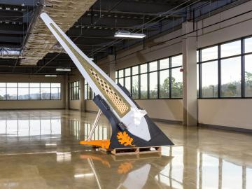
In the shifting landscape of global manufacturing, American ingenuity is once again giving U.S companies an edge with radical productivity improvements as a result of advanced materials and robotic systems developed at the Department of Energy’s Manufacturing Demonstration Facility (MDF) at Oak Ridge National Laboratory.
![Strain-tolerant, triangular, monolayer crystals of WS2 were grown on SiO2 substrates patterned with donut-shaped pillars, as shown in scanning electron microscope (bottom) and atomic force microscope (middle) image elements.](/sites/default/files/styles/list_page_thumbnail/public/2019-06/Image%201_5.jpg?h=62c69fe2&itok=NWF1WS0c)
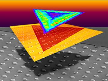
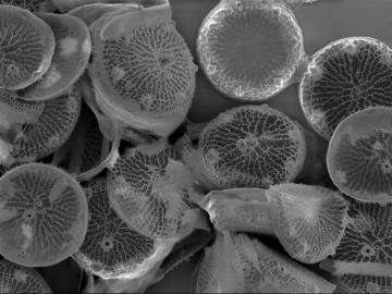
A team led by scientists at the Department of Energy’s Oak Ridge National Laboratory explored how atomically thin two-dimensional (2D) crystals can grow over 3D objects and how the curvature of those objects can stretch and strain the