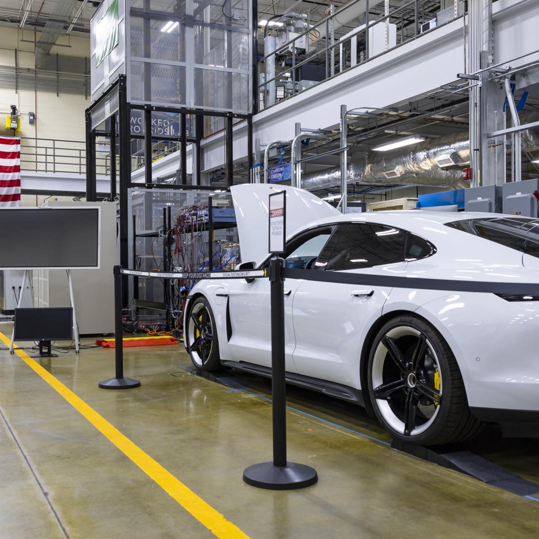
A surfactant template guides the self-assembly of functional polymer structures in an aqueous solution. Image credit: Oak Ridge National Laboratory, U.S. Dept. of Energy; image by Youngkyu Han and Renee Manning.
The efficiency of solar cells depends on precise engineering of polymers that assemble into films 1,000 times thinner than a human hair. Today, formation of that polymer assembly requires solvents that can harm the environment, but scientists at the Department of En...
An ORNL-University of Rome study has delivered direct evidence of high-temperature superconductivity at the interface of two insulating oxide materials. Electron microscopy at ORNL showed that superconductivity arises from oxygen ions (circled in white) t
Electron microscopy at the Department of Energy’s Oak Ridge National Laboratory is pointing researchers closer to the development of ultra-thin materials that transfer electrons with no resistance at relatively high temperatures. The study delivers direct evidence of high-tem...
Default image of ORNL entry sign
Some of the 300 million tires discarded each year in the United States alone could be used in supercapacitors for vehicles and the electric grid using a technology developed at the Department of Energy’s Oak Ridge National Laboratory and Drexel University. By em...
OAK RIDGE, Tenn., Sept. 14, 2015 – A catalyst being developed by researchers at the Department of Energy’s Oak Ridge National Laboratory could overcome one of the key obstacles still preventing automobile engines from running more cleanly and efficiently.

A catalyst being developed by researchers at the Department of Energy’s Oak Ridge National Laboratory could overcome one of the key obstacles still preventing automobile engines from running more cleanly and efficiently. The mixed oxide catalyst could solve the ...

Secretary of Commerce Penny Pritzker inspects the Institute for Advanced Composites Manufacturing Innovation (IACMI) at Oak Ridge National Laboratory, hosted by Craig Blue, IACMI’s chief executive officer. (Jason Richards photo).
Secretary of Commerce Penny Pritzker visited the new Institute for Advanced Composites Manufacturing Innovation (IACMI) at Oak Ridge National Laboratory’s Manufacturing Demonstration Facility, praising the advances in manufacturing technology taking place in East T...
Material dissolved in the liquid at the port tip is immediately transported into the mass spectrometer, ionized, detected and characterized.
In mere seconds, a system developed at the Department of Energy’s Oak Ridge National Laboratory can identify and characterize a solid or liquid sample, providing a valuable tool with applications in material science, forensics, pharmaceuticals, biology and chemistry.
The “Big, Deep and Smart Data Analytics in Materials Imaging” workshop

In the Stone, Bronze and Iron Ages, the state of the art of materials science defined technology’s zenith and accelerated economies. Now, in the Information Age, data is beginning to drive the development of advanced materials, from photovoltaics for solar energy and superconductors for efficient el...

Default image of ORNL entry sign

A new technology developed by the U.S. Department of Energy’s Critical Materials Institute that aids in the recycling, recovery and extraction of rare earth minerals has been licensed to U.S. Rare Earths, Inc.

Developed by Oak Ridge National Laboratory researchers, CIRFT bends and vibrates used nuclear fuel rod segments to test the impact of normal traveling conditions—before the fuel rods ever leave the premises.
Moving rods of spent nuclear fuel (SNF) to interim storage or a geologic repository requires road or rail travel. Although a heavy shielding cask protects the rods, long distance transportation subjects SNF to vibrations, sudden movements and other potentially agitating for...
Complex, scalable arrays of semiconductor heterojunctions—promising building blocks for future electronics.
Semiconductors, metals and insulators must be integrated to make the transistors that are the electronic building blocks of your smartphone, computer and other microchip-enabled devices. Today’s transistors are miniscule—a mere 10 nanometers wide—and forme...