![Sphere that has the top right fourth removed (exposed) Colors from left are orange, dark blue with orange dots, light blue with horizontal lines, then black. Inside the exposure is green and black with boxes.](/sites/default/files/styles/featured_square_large/public/2024-06/slicer.jpg?h=56311bf6&itok=bCZz09pJ)
Filter News
Area of Research
- (-) Materials (30)
- Biology and Environment (39)
- Biology and Soft Matter (1)
- Clean Energy (20)
- Climate and Environmental Systems (2)
- Computational Biology (1)
- Computational Engineering (2)
- Computer Science (5)
- Fusion and Fission (2)
- Materials for Computing (9)
- Mathematics (1)
- National Security (11)
- Neutron Science (11)
- Nuclear Science and Technology (1)
- Quantum information Science (7)
- Supercomputing (53)
News Type
News Topics
- (-) Artificial Intelligence (4)
- (-) Nanotechnology (16)
- (-) Physics (13)
- (-) Quantum Science (1)
- 3-D Printing/Advanced Manufacturing (10)
- Advanced Reactors (2)
- Big Data (2)
- Bioenergy (3)
- Biomedical (4)
- Buildings (2)
- Chemical Sciences (11)
- Clean Water (3)
- Composites (6)
- Computer Science (9)
- Coronavirus (2)
- Critical Materials (5)
- Cybersecurity (1)
- Decarbonization (2)
- Energy Storage (13)
- Environment (7)
- Exascale Computing (1)
- Fusion (4)
- Grid (2)
- High-Performance Computing (1)
- Isotopes (8)
- Machine Learning (2)
- Materials (31)
- Materials Science (36)
- Mathematics (1)
- Microscopy (12)
- Molten Salt (1)
- Neutron Science (13)
- Nuclear Energy (12)
- Partnerships (3)
- Polymers (10)
- Quantum Computing (2)
- Security (1)
- Space Exploration (2)
- Summit (1)
- Sustainable Energy (5)
- Transformational Challenge Reactor (2)
- Transportation (10)
Media Contacts
![Scanning probe microscopes use an atom-sharp tip—only a few nanometers thick—to image materials on a nanometer length scale. The probe tip, invisible to the eye, is attached to a cantilever (pictured) that moves across material surfaces like the tone arm on a record player. Credit: Genevieve Martin/Oak Ridge National Laboratory; U.S. Dept. of Energy.](/sites/default/files/styles/list_page_thumbnail/public/2020-01/2019-P15115.jpg?h=c6980913&itok=o69jyoNw)
Liam Collins was drawn to study physics to understand “hidden things” and honed his expertise in microscopy so that he could bring them to light.
![ORNL-developed cryogenic memory cell circuit designs fabricated onto these small chips by SeeQC, a superconducting technology company, successfully demonstrated read, write and reset memory functions. Credit: Carlos Jones/Oak Ridge National Laboratory, U.S. Dept. of Energy](/sites/default/files/styles/list_page_thumbnail/public/2020-01/2019-P17636.png?h=39b94f55&itok=udTwXJwT)
Scientists at have experimentally demonstrated a novel cryogenic, or low temperature, memory cell circuit design based on coupled arrays of Josephson junctions, a technology that may be faster and more energy efficient than existing memory devices.
![The students analyzed diatom images like this one to compare wild and genetically modified strains of these organisms. Credit: Alison Pawlicki/Oak Ridge National Laboratory, US Department of Energy.](/sites/default/files/styles/list_page_thumbnail/public/2019-11/RI4362007.png?h=37702503&itok=9lQReLRe)
Students often participate in internships and receive formal training in their chosen career fields during college, but some pursue professional development opportunities even earlier.
![Researchers at the Center for Nanophase Materials Sciences demonstrated an insect-inspired, mechanical gyroscope to advance motion sensing capabilities in consumer-sized applications. Credit: Jill Hemman/Oak Ridge National Laboratory, U.S Dept. of Energy](/sites/default/files/styles/list_page_thumbnail/public/2019-11/19-G01034_Image_Lavrik.jpg?h=9bd356d5&itok=tDYVRTH5)
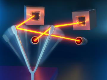
Researchers at ORNL and the National Renewable Energy Laboratory took inspiration from flying insects to demonstrate a miniaturized gyroscope, a special sensor used in navigation technologies.
![Desalination process](/sites/default/files/styles/list_page_thumbnail/public/2019-07/hydrophopicDesal04_0.jpg?h=5473d993&itok=bUBkpGOa)
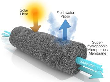
A new method developed at Oak Ridge National Laboratory improves the energy efficiency of a desalination process known as solar-thermal evaporation.
![Materials—Engineering heat transport](/sites/default/files/styles/list_page_thumbnail/public/2019-05/Materials-Engineering_heat_transport.png?h=abd215d5&itok=PJPSWa9s)
Scientists have discovered a way to alter heat transport in thermoelectric materials, a finding that may ultimately improve energy efficiency as the materials
![Physics_silicon-detectors.jpg](/sites/default/files/styles/list_page_thumbnail/public/Physics_silicon-detectors.jpg?h=c920d705&itok=Q1fP5ZTi)
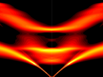
Physicists turned to the “doubly magic” tin isotope Sn-132, colliding it with a target at Oak Ridge National Laboratory to assess its properties as it lost a neutron to become Sn-131.
![B_Hudak_ORNL.jpg B_Hudak_ORNL.jpg](/sites/default/files/styles/list_page_thumbnail/public/B_Hudak_ORNL.jpg?itok=Os5uKm-q)
An Oak Ridge National Laboratory-led team used a scanning transmission electron microscope to selectively position single atoms below a crystal’s surface for the first time.
![Schematic drawing of the boron nitride cell. Credit: University of Illinois at Chicago. Schematic drawing of the boron nitride cell. Credit: University of Illinois at Chicago.](/sites/default/files/styles/list_page_thumbnail/public/news/images/schematic1.jpg?itok=iYCttAg3)
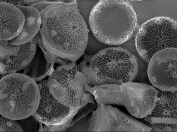
A new microscopy technique developed at the University of Illinois at Chicago allows researchers to visualize liquids at the nanoscale level — about 10 times more resolution than with traditional transmission electron microscopy — for the first time. By trapping minute amounts of...
![An ORNL-led team used scanning transmission electron microscopy to observed atomic transformations on the edges of pores in a two-dimensional transition metal dichalcogenide. The controlled production of nanopores with stable atomic edge structures may en An ORNL-led team used scanning transmission electron microscopy to observed atomic transformations on the edges of pores in a two-dimensional transition metal dichalcogenide. The controlled production of nanopores with stable atomic edge structures may en](/sites/default/files/styles/list_page_thumbnail/public/news/images/03%20-%20MoWSe2%20StoryTip%20Fig_PRINT%20r1.jpg?itok=cT1gasG8)
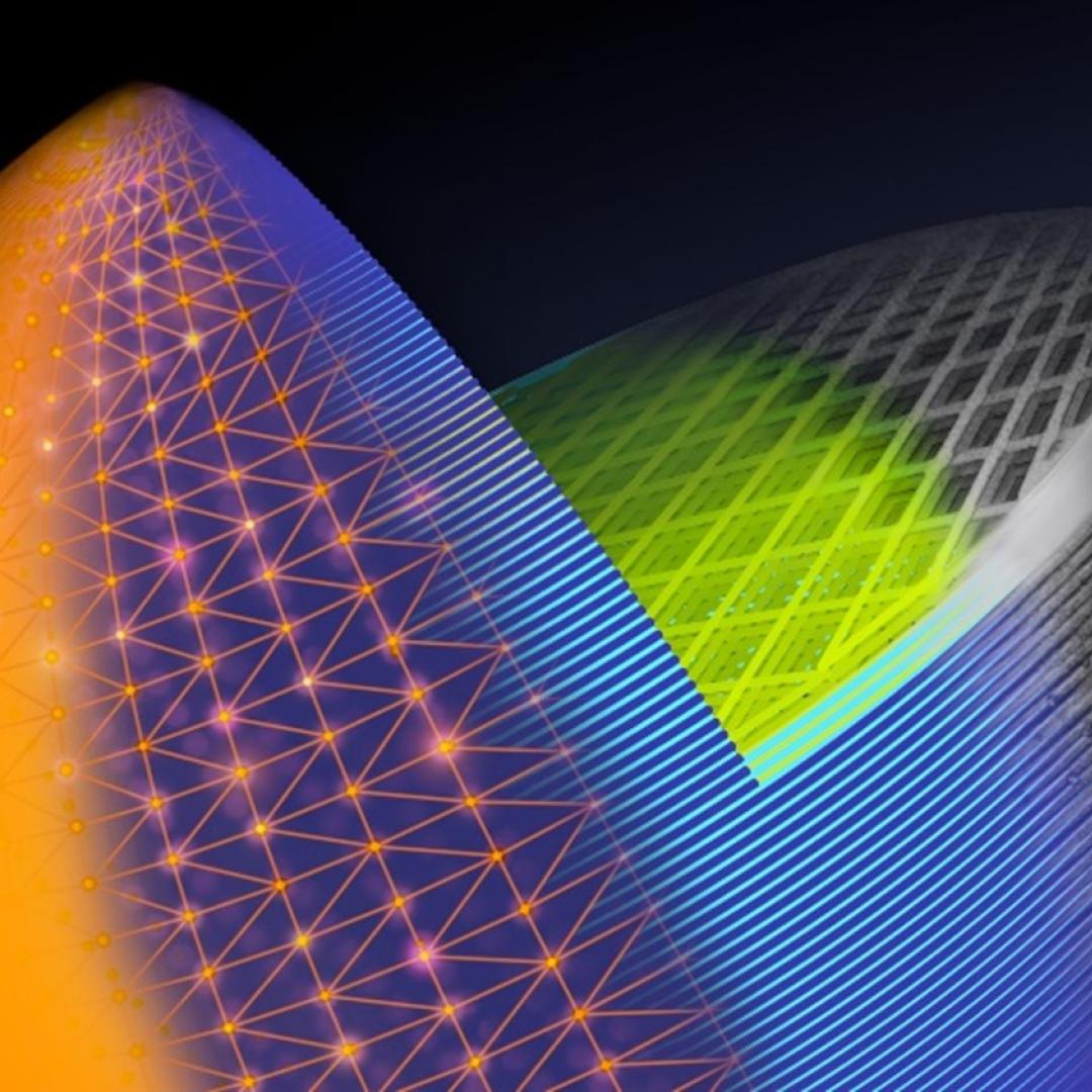
An Oak Ridge National Laboratory–led team has learned how to engineer tiny pores embellished with distinct edge structures inside atomically-thin two-dimensional, or 2D, crystals. The 2D crystals are envisioned as stackable building blocks for ultrathin electronics and other advance...