
Updated software improves slicing for large-format 3D printing

Researchers at ORNL used quantum optics to advance state-of-the-art microscopy and illuminate a path to detecting material properties with greater sensitivity than is possible with traditional tools.

Five researchers at the Department of Energy’s Oak Ridge National Laboratory have been named ORNL Corporate Fellows in recognition of significant career accomplishments and continued leadership in their scientific fields.
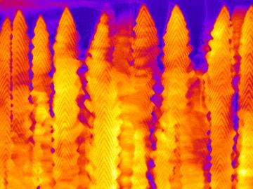
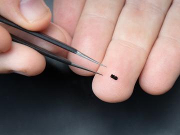
An ORNL team used a simple process to implant atoms precisely into the top layers of ultra-thin crystals, yielding two-sided structures with different chemical compositions.
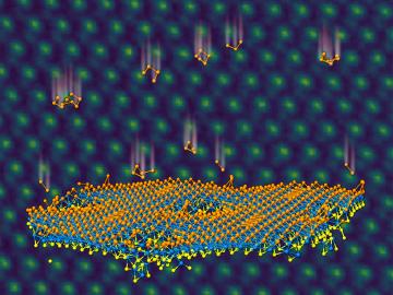
A team led by the Department of Energy’s Oak Ridge National Laboratory synthesized a tiny structure with high surface area and discovered how its unique architecture drives ions across interfaces to transport energy or information.

For the second year in a row, a team from the Department of Energy’s Oak Ridge and Los Alamos national laboratories led a demonstration hosted by EPB, a community-based utility and telecommunications company serving Chattanooga, Tennessee.

Rigoberto “Gobet” Advincula has been named Governor’s Chair of Advanced and Nanostructured Materials at Oak Ridge National Laboratory and the University of Tennessee.
Liam Collins was drawn to study physics to understand “hidden things” and honed his expertise in microscopy so that he could bring them to light.

Kathy McCarthy has been named director of the US ITER Project Office at the Department of Energy’s Oak Ridge National Laboratory, effective March 2020.

A joint research team from Google Inc., NASA Ames Research Center, and the Department of Energy’s Oak Ridge National Laboratory has demonstrated that a quantum computer can outperform a classical computer
The U.S. Department of Energy announced funding for 12 projects with private industry to enable collaboration with DOE national laboratories on overcoming challenges in fusion energy development.