![Sphere that has the top right fourth removed (exposed) Colors from left are orange, dark blue with orange dots, light blue with horizontal lines, then black. Inside the exposure is green and black with boxes.](/sites/default/files/styles/featured_square_large/public/2024-06/slicer.jpg?h=56311bf6&itok=bCZz09pJ)
Filter News
Area of Research
- (-) Isotope Development and Production (1)
- (-) Materials (65)
- Biology and Environment (26)
- Clean Energy (26)
- Computational Engineering (1)
- Computer Science (1)
- Energy Frontier Research Centers (1)
- Fusion and Fission (8)
- Isotopes (15)
- Materials Characterization (1)
- Materials for Computing (6)
- Materials Under Extremes (1)
- National Security (5)
- Neutron Science (18)
- Nuclear Science and Technology (3)
- Supercomputing (15)
News Type
News Topics
- (-) Biomedical (3)
- (-) Isotopes (5)
- (-) Materials Science (42)
- (-) Nanotechnology (25)
- (-) Partnerships (8)
- (-) Renewable Energy (1)
- 3-D Printing/Advanced Manufacturing (13)
- Advanced Reactors (1)
- Artificial Intelligence (4)
- Bioenergy (9)
- Biology (4)
- Buildings (2)
- Chemical Sciences (22)
- Climate Change (5)
- Composites (3)
- Computer Science (8)
- Coronavirus (2)
- Critical Materials (8)
- Cybersecurity (3)
- Decarbonization (4)
- Energy Storage (20)
- Environment (8)
- Exascale Computing (1)
- Frontier (2)
- Fusion (3)
- Grid (2)
- High-Performance Computing (2)
- ITER (1)
- Machine Learning (2)
- Materials (41)
- Microscopy (15)
- Molten Salt (2)
- National Security (3)
- Net Zero (1)
- Neutron Science (20)
- Nuclear Energy (5)
- Physics (20)
- Polymers (8)
- Quantum Computing (2)
- Quantum Science (10)
- Security (1)
- Space Exploration (1)
- Summit (1)
- Sustainable Energy (7)
- Transformational Challenge Reactor (1)
- Transportation (4)
Media Contacts
![Selenium atoms, represented by orange, implant in a monolayer of blue tungsten and yellow sulfur to form a Janus layer. In the background, electron microscopy confirms atomic positions. Credit: Oak Ridge National Laboratory, U.S. Dept. of Energy](/sites/default/files/styles/list_page_thumbnail/public/2020-06/Cover%20Art%20nn-2019-10196k_8_0.jpg?h=97102f31&itok=F-JpEvZ2)
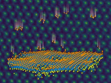
An ORNL team used a simple process to implant atoms precisely into the top layers of ultra-thin crystals, yielding two-sided structures with different chemical compositions.
![Yanwen Zhang](/sites/default/files/styles/list_page_thumbnail/public/2020-06/2018-P06460.png?h=854a7be2&itok=i4P7m_Rx)
In the search to create materials that can withstand extreme radiation, Yanwen Zhang, a researcher at the Department of Energy’s Oak Ridge National Laboratory, says that materials scientists must think outside the box.
![A nanobrush made by pulsed laser deposition of CeO2 and Y2O3 with dim and bright bands, respectively, is seen in cross-section with scanning transmission electron microscopy. Credit: Oak Ridge National Laboratory, U.S. Dept. of Energy](/sites/default/files/styles/list_page_thumbnail/public/2020-06/HAADF-137804_FIRE_scale_0.jpg?h=ea2c671e&itok=8URQqQi6)
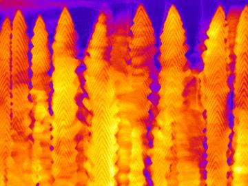
A team led by the Department of Energy’s Oak Ridge National Laboratory synthesized a tiny structure with high surface area and discovered how its unique architecture drives ions across interfaces to transport energy or information.
![Polymer self-assembly at the liquid-liquid interface in real time](/sites/default/files/styles/list_page_thumbnail/public/2020-02/descent.png?h=d1cb525d&itok=rz3eSM-H)
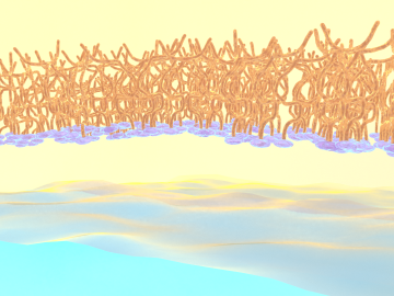
OAK RIDGE, Tenn., Feb. 27, 2020 — Researchers at Oak Ridge National Laboratory and the University of Tennessee achieved a rare look at the inner workings of polymer self-assembly at an oil-water interface to advance materials for neuromorphic computing and bio-inspired technologies.
![Closely spaced hydrogen atoms could facilitate superconductivity in ambient conditions](/sites/default/files/styles/list_page_thumbnail/public/2020-02/Closely_spaced_hydrogen_atoms-correct.png?h=6a4c2577&itok=GBnxpWls)
An international team of researchers has discovered the hydrogen atoms in a metal hydride material are much more tightly spaced than had been predicted for decades — a feature that could possibly facilitate superconductivity at or near room temperature and pressure.
![Gobet_Advincula Portrait](/sites/default/files/styles/list_page_thumbnail/public/2020-02/2020-P00191.png?h=8f9cfe54&itok=MA0hIqj6)
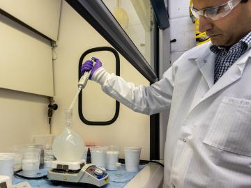
Rigoberto “Gobet” Advincula has been named Governor’s Chair of Advanced and Nanostructured Materials at Oak Ridge National Laboratory and the University of Tennessee.
![Scanning probe microscopes use an atom-sharp tip—only a few nanometers thick—to image materials on a nanometer length scale. The probe tip, invisible to the eye, is attached to a cantilever (pictured) that moves across material surfaces like the tone arm on a record player. Credit: Genevieve Martin/Oak Ridge National Laboratory; U.S. Dept. of Energy.](/sites/default/files/styles/list_page_thumbnail/public/2020-01/2019-P15115.jpg?h=c6980913&itok=o69jyoNw)
Liam Collins was drawn to study physics to understand “hidden things” and honed his expertise in microscopy so that he could bring them to light.
![Representatives from The University of Toledo and the U.S. Department of Energy’s Oak Ridge National Laboratory (ORNL) in Tennessee are teaming up to conduct collaborative automotive materials research.” Credit: University of Toledo](/sites/default/files/styles/list_page_thumbnail/public/2019-10/Oak%20Ridge%20Nat%20Lab%20group%20photo_0.jpeg?h=1e7f2295&itok=pITK15-V)
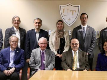
ORNL and The University of Toledo have entered into a memorandum of understanding for collaborative research.
![low-cost material can be used as an additive to increase thermal insulation performance](/sites/default/files/styles/list_page_thumbnail/public/2019-09/2019-P09265_0.jpg?h=036a71b7&itok=tVT2cC3V)
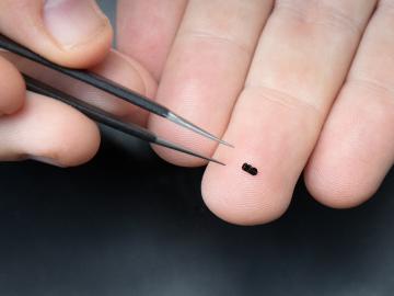
Quanex Building Products has signed a non-exclusive agreement to license a method to produce insulating material from ORNL. The low-cost material can be used as an additive to increase thermal insulation performance and improve energy efficiency when applied to a variety of building products.
![Strain-tolerant, triangular, monolayer crystals of WS2 were grown on SiO2 substrates patterned with donut-shaped pillars, as shown in scanning electron microscope (bottom) and atomic force microscope (middle) image elements.](/sites/default/files/styles/list_page_thumbnail/public/2019-06/Image%201_5.jpg?h=62c69fe2&itok=NWF1WS0c)
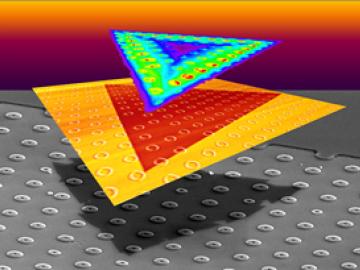
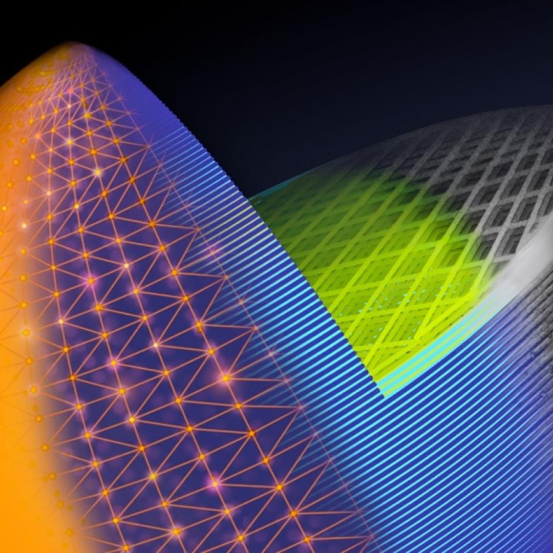
A team led by scientists at the Department of Energy’s Oak Ridge National Laboratory explored how atomically thin two-dimensional (2D) crystals can grow over 3D objects and how the curvature of those objects can stretch and strain the