![Sphere that has the top right fourth removed (exposed) Colors from left are orange, dark blue with orange dots, light blue with horizontal lines, then black. Inside the exposure is green and black with boxes.](/sites/default/files/styles/featured_square_large/public/2024-06/slicer.jpg?h=56311bf6&itok=bCZz09pJ)
Filter News
Area of Research
- (-) Materials (22)
- (-) Neutron Science (3)
- Advanced Manufacturing (1)
- Biology and Environment (3)
- Clean Energy (7)
- Computational Engineering (1)
- Computer Science (3)
- Fusion and Fission (2)
- Isotopes (10)
- Materials for Computing (3)
- National Security (9)
- Nuclear Science and Technology (4)
- Quantum information Science (1)
- Supercomputing (3)
News Type
News Topics
- (-) Isotopes (2)
- (-) Nanotechnology (13)
- (-) Physics (8)
- (-) Space Exploration (2)
- 3-D Printing/Advanced Manufacturing (6)
- Advanced Reactors (1)
- Artificial Intelligence (1)
- Bioenergy (3)
- Biomedical (4)
- Buildings (1)
- Chemical Sciences (7)
- Clean Water (1)
- Composites (4)
- Computer Science (1)
- Coronavirus (1)
- Critical Materials (5)
- Decarbonization (1)
- Energy Storage (10)
- Environment (2)
- Fusion (3)
- Materials (17)
- Materials Science (26)
- Microscopy (9)
- Molten Salt (1)
- Neutron Science (30)
- Nuclear Energy (6)
- Polymers (8)
- Quantum Computing (2)
- Quantum Science (2)
- Sustainable Energy (3)
- Transportation (8)
Media Contacts
![B_Hudak_ORNL.jpg B_Hudak_ORNL.jpg](/sites/default/files/styles/list_page_thumbnail/public/B_Hudak_ORNL.jpg?itok=Os5uKm-q)
An Oak Ridge National Laboratory-led team used a scanning transmission electron microscope to selectively position single atoms below a crystal’s surface for the first time.
![Sergei Kalinin, director of the Institute for Functional Imaging of Materials at Oak Ridge National Laboratory, convenes experts in microscopy and computing to gain scientific insights that will inform design of advanced materials for energy and informati Sergei Kalinin, director of the Institute for Functional Imaging of Materials at Oak Ridge National Laboratory, convenes experts in microscopy and computing to gain scientific insights that will inform design of advanced materials for energy and informati](/sites/default/files/styles/list_page_thumbnail/public/news/images/2018-P00854%20%28002%29.jpg?itok=UfhMWf3G)
Sergei Kalinin of the Department of Energy’s Oak Ridge National Laboratory knows that seeing something is not the same as understanding it. As director of ORNL’s Institute for Functional Imaging of Materials, he convenes experts in microscopy and computing to gain scientific insigh...
![An ORNL-led team used scanning transmission electron microscopy to observed atomic transformations on the edges of pores in a two-dimensional transition metal dichalcogenide. The controlled production of nanopores with stable atomic edge structures may en An ORNL-led team used scanning transmission electron microscopy to observed atomic transformations on the edges of pores in a two-dimensional transition metal dichalcogenide. The controlled production of nanopores with stable atomic edge structures may en](/sites/default/files/styles/list_page_thumbnail/public/news/images/03%20-%20MoWSe2%20StoryTip%20Fig_PRINT%20r1.jpg?itok=cT1gasG8)
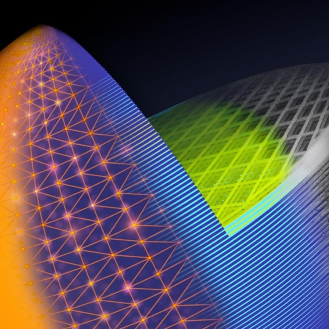
An Oak Ridge National Laboratory–led team has learned how to engineer tiny pores embellished with distinct edge structures inside atomically-thin two-dimensional, or 2D, crystals. The 2D crystals are envisioned as stackable building blocks for ultrathin electronics and other advance...
![Illustration of satellite in front of glowing orange celestial body](/sites/default/files/styles/list_page_thumbnail/public/NASA_Parker_Solar_Probe_rendering.jpg?h=90c266c4&itok=KqHQKRNt)
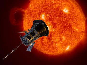
A shield assembly that protects an instrument measuring ion and electron fluxes for a NASA mission to touch the Sun was tested in extreme experimental environments at Oak Ridge National Laboratory—and passed with flying colors. Components aboard Parker Solar Probe, which will endure th...