

Scientists at Oak Ridge National Laboratory and the University of Tennessee designed and demonstrated a method to make carbon-based materials that can be used as electrodes compatible with a specific semiconductor circuitry.
An all-in-one experimental platform developed at Oak Ridge National Laboratory’s Center for Nanophase Materials Sciences accelerates research on promising materials for future technologies.
Researchers at ORNL and the National Renewable Energy Laboratory took inspiration from flying insects to demonstrate a miniaturized gyroscope, a special sensor used in navigation technologies.
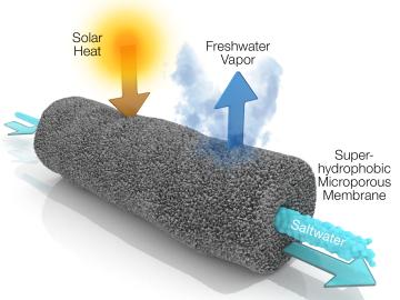
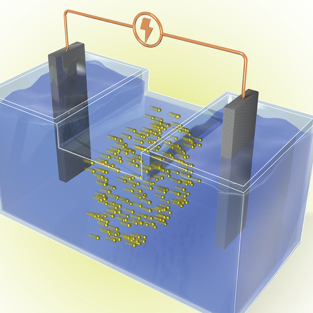
A new method developed at Oak Ridge National Laboratory improves the energy efficiency of a desalination process known as solar-thermal evaporation.
![2018-P07635 BL-6 user - Univ of Guelph-6004R_sm[2].jpg](/sites/default/files/styles/list_page_thumbnail/public/2018-P07635%20BL-6%20user%20-%20Univ%20of%20Guelph-6004R_sm%5B2%5D.jpg?itok=DUdZNt_q "2018-P07635 BL-6 user - Univ of Guelph-6004R_sm[2].jpg")
A team of scientists, led by University of Guelph professor John Dutcher, are using neutrons at ORNL’s Spallation Neutron Source to unlock the secrets of natural nanoparticles that could be used to improve medicines.

An Oak Ridge National Laboratory-led team used a scanning transmission electron microscope to selectively position single atoms below a crystal’s surface for the first time.

An Oak Ridge National Laboratory–led team has learned how to engineer tiny pores embellished with distinct edge structures inside atomically-thin two-dimensional, or 2D, crystals. The 2D crystals are envisioned as stackable building blocks for ultrathin electronics and other advance...