Updated software improves slicing for large-format 3D printing
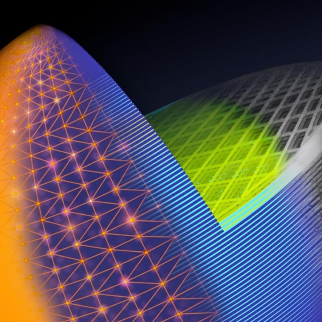
A team led by scientists at the Department of Energy’s Oak Ridge National Laboratory explored how atomically thin two-dimensional (2D) crystals can grow over 3D objects and how the curvature of those objects can stretch and strain the

OAK RIDGE, Tenn., May 7, 2019—Energy Secretary Rick Perry, Congressman Chuck Fleischmann and lab officials today broke ground on a multipurpose research facility that will provide state-of-the-art laboratory space
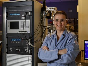
Vera Bocharova at the Department of Energy’s Oak Ridge National Laboratory investigates the structure and dynamics of soft materials—polymer nanocomposites, polymer electrolytes and biological macromolecules—to advance materials and technologies for energy, medicine and other applications.

OAK RIDGE, Tenn., Feb. 8, 2019—The Department of Energy’s Oak Ridge National Laboratory has named Sean Hearne director of the Center for Nanophase Materials Sciences. The center is a DOE Office of Science User Facility that brings world-leading resources and capabilities to the nanoscience resear...

OAK RIDGE, Tenn., Jan. 31, 2019—A new electron microscopy technique that detects the subtle changes in the weight of proteins at the nanoscale—while keeping the sample intact—could open a new pathway for deeper, more comprehensive studies of the basic building blocks of life.

An Oak Ridge National Laboratory-led team used a scanning transmission electron microscope to selectively position single atoms below a crystal’s surface for the first time.

Scientists at the Department of Energy’s Oak Ridge National Laboratory induced a two-dimensional material to cannibalize itself for atomic “building blocks” from which stable structures formed. The findings, reported in Nature Communications, provide insights that ...

Sergei Kalinin of the Department of Energy’s Oak Ridge National Laboratory knows that seeing something is not the same as understanding it. As director of ORNL’s Institute for Functional Imaging of Materials, he convenes experts in microscopy and computing to gain scientific insigh...

A new microscopy technique developed at the University of Illinois at Chicago allows researchers to visualize liquids at the nanoscale level — about 10 times more resolution than with traditional transmission electron microscopy — for the first time. By trapping minute amounts of...

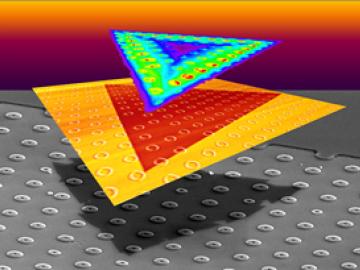
An Oak Ridge National Laboratory–led team has learned how to engineer tiny pores embellished with distinct edge structures inside atomically-thin two-dimensional, or 2D, crystals. The 2D crystals are envisioned as stackable building blocks for ultrathin electronics and other advance...