ORNL-developed cryogenic memory cell circuit designs fabricated onto these small chips by SeeQC, a superconducting technology company, successfully demonstrated read, write and reset memory functions. Credit: Carlos Jones/Oak Ridge National Laboratory, U.S. Dept. of Energy

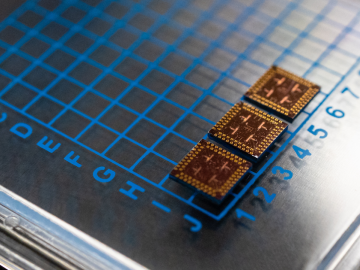
Scientists at have experimentally demonstrated a novel cryogenic, or low temperature, memory cell circuit design based on coupled arrays of Josephson junctions, a technology that may be faster and more energy efficient than existing memory devices.

Strain-tolerant, triangular, monolayer crystals of WS2 were grown on SiO2 substrates patterned with donut-shaped pillars, as shown in scanning electron microscope (bottom) and atomic force microscope (middle) image elements.

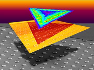
A team led by scientists at the Department of Energy’s Oak Ridge National Laboratory explored how atomically thin two-dimensional (2D) crystals can grow over 3D objects and how the curvature of those objects can stretch and strain the 

Pictured in this early conceptual drawing, the Translational Research Capability planned for Oak Ridge National Laboratory will follow the design of research facilities constructed during the laboratory’s modernization campaign.

OAK RIDGE, Tenn., May 7, 2019—Energy Secretary Rick Perry, Congressman Chuck Fleischmann and lab officials today broke ground on a multipurpose research facility that will provide state-of-the-art laboratory space