Updated software improves slicing for large-format 3D printing
An all-in-one experimental platform developed at Oak Ridge National Laboratory’s Center for Nanophase Materials Sciences accelerates research on promising materials for future technologies.
From materials science and earth system modeling to quantum information science and cybersecurity, experts in many fields run simulations and conduct experiments to collect the abundance of data necessary for scientific progress.

Five researchers at the Department of Energy’s Oak Ridge National Laboratory have been named ORNL Corporate Fellows in recognition of significant career accomplishments and continued leadership in their scientific fields.
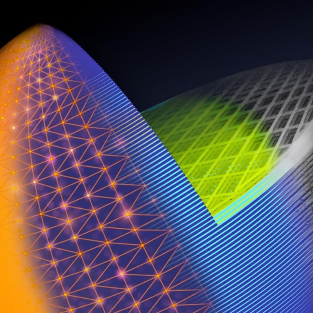
An ORNL team used a simple process to implant atoms precisely into the top layers of ultra-thin crystals, yielding two-sided structures with different chemical compositions.
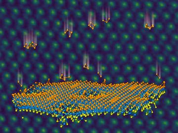
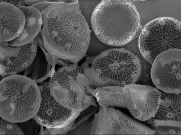
A team led by the Department of Energy’s Oak Ridge National Laboratory synthesized a tiny structure with high surface area and discovered how its unique architecture drives ions across interfaces to transport energy or information.

Rigoberto “Gobet” Advincula has been named Governor’s Chair of Advanced and Nanostructured Materials at Oak Ridge National Laboratory and the University of Tennessee.
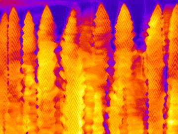
Liam Collins was drawn to study physics to understand “hidden things” and honed his expertise in microscopy so that he could bring them to light.
Students often participate in internships and receive formal training in their chosen career fields during college, but some pursue professional development opportunities even earlier.

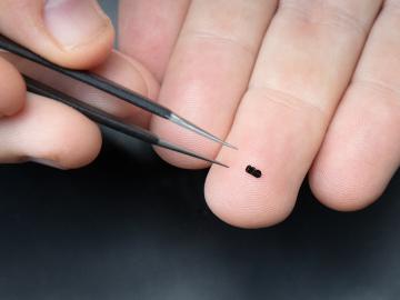
Researchers at ORNL and the National Renewable Energy Laboratory took inspiration from flying insects to demonstrate a miniaturized gyroscope, a special sensor used in navigation technologies.
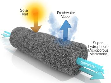
A new method developed at Oak Ridge National Laboratory improves the energy efficiency of a desalination process known as solar-thermal evaporation.