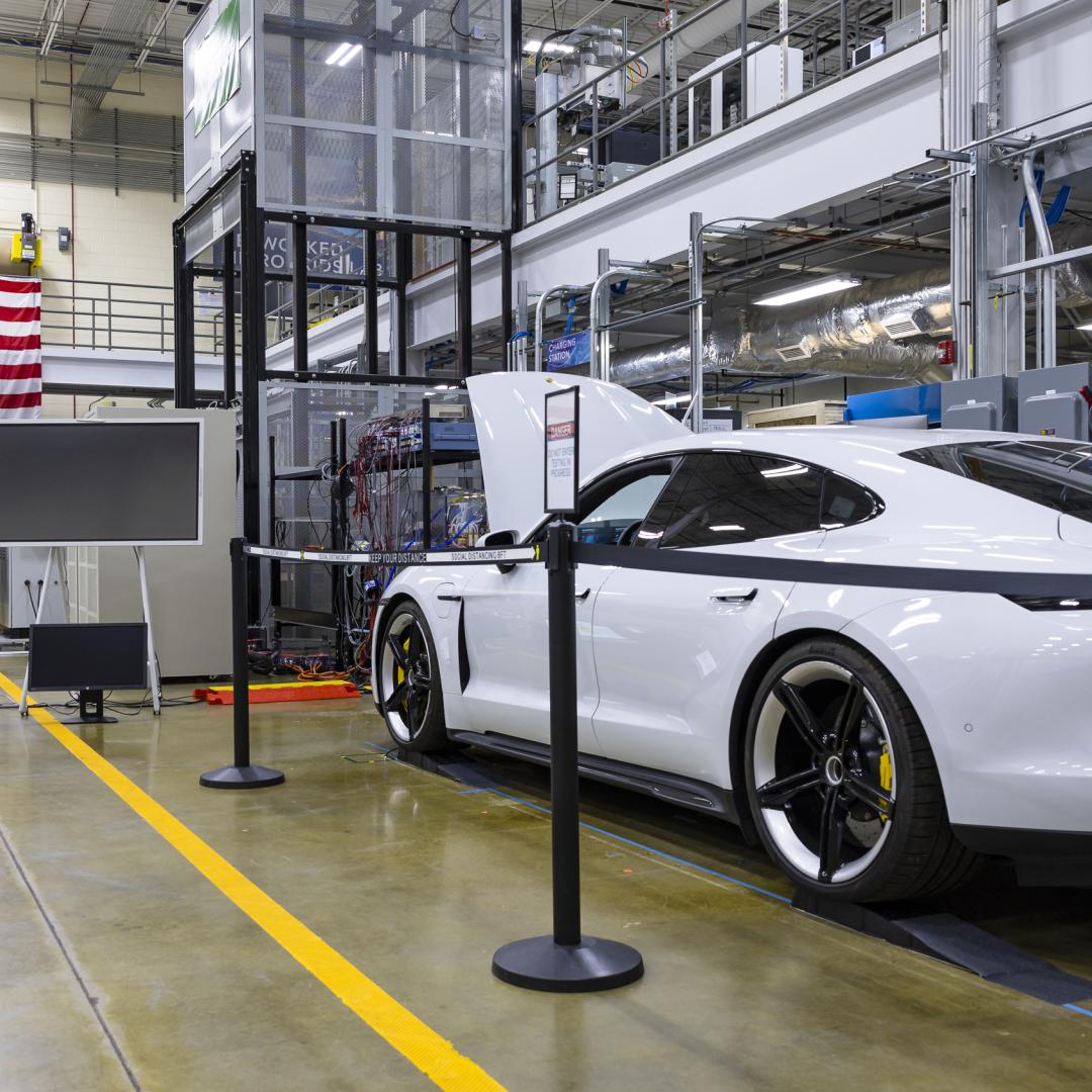
Polyphase wireless power transfer system achieves 270-kilowatt charge, s...

Rigoberto “Gobet” Advincula has been named Governor’s Chair of Advanced and Nanostructured Materials at Oak Ridge National Laboratory and the University of Tennessee.
Liam Collins was drawn to study physics to understand “hidden things” and honed his expertise in microscopy so that he could bring them to light.
Scientists at have experimentally demonstrated a novel cryogenic, or low temperature, memory cell circuit design based on coupled arrays of Josephson junctions, a technology that may be faster and more energy efficient than existing memory devices.

Researchers across the scientific spectrum crave data, as it is essential to understanding the natural world and, by extension, accelerating scientific progress.
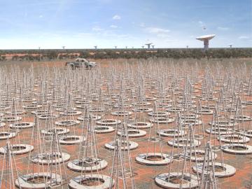
For nearly three decades, scientists and engineers across the globe have worked on the Square Kilometre Array (SKA), a project focused on designing and building the world’s largest radio telescope. Although the SKA will collect enormous amounts of precise astronomical data in record time, scientific breakthroughs will only be possible with systems able to efficiently process that data.
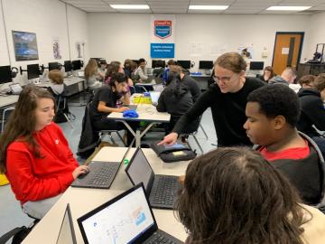
ORNL computer scientist Catherine Schuman returned to her alma mater, Harriman High School, to lead Hour of Code activities and talk to students about her job as a researcher.
Students often participate in internships and receive formal training in their chosen career fields during college, but some pursue professional development opportunities even earlier.
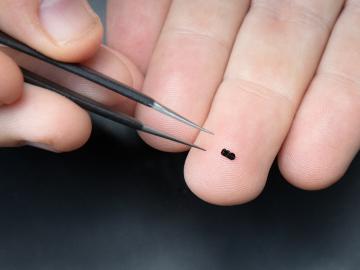
Researchers at ORNL and the National Renewable Energy Laboratory took inspiration from flying insects to demonstrate a miniaturized gyroscope, a special sensor used in navigation technologies.
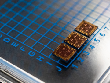
IDEMIA Identity & Security USA has licensed an advanced optical array developed at Oak Ridge National Laboratory. The portable technology can be used to help identify individuals in challenging outdoor conditions.

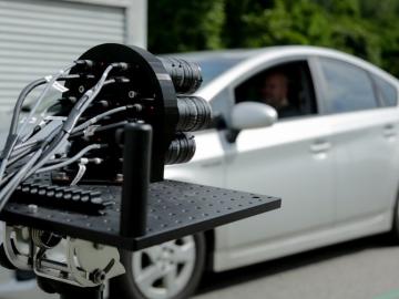
Oak Ridge National Laboratory is training next-generation cameras called dynamic vision sensors, or DVS, to interpret live information—a capability that has applications in robotics and could improve autonomous vehicle sensing.
