Updated software improves slicing for large-format 3D printing
Scientists at Oak Ridge National Laboratory and the University of Tennessee designed and demonstrated a method to make carbon-based materials that can be used as electrodes compatible with a specific semiconductor circuitry.
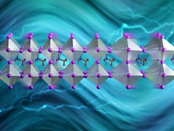
Led by ORNL and the University of Tennessee, Knoxville, a study of a solar-energy material with a bright future revealed a way to slow phonons, the waves that transport heat.

The combination of bioenergy with carbon capture and storage could cost-effectively sequester hundreds of millions of metric tons per year of carbon dioxide in the United States, making it a competitive solution for carbon management, according to a new analysis by ORNL scientists.
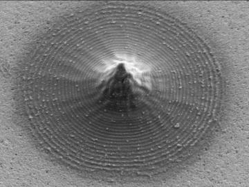
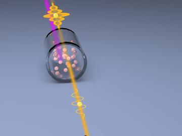
Scientists at ORNL and the University of Nebraska have developed an easier way to generate electrons for nanoscale imaging and sensing, providing a useful new tool for material science, bioimaging and fundamental quantum research.
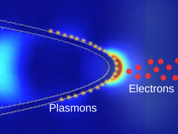
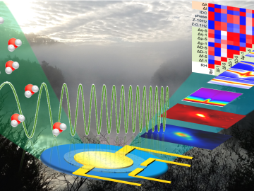
Researchers at ORNL used quantum optics to advance state-of-the-art microscopy and illuminate a path to detecting material properties with greater sensitivity than is possible with traditional tools.
An all-in-one experimental platform developed at Oak Ridge National Laboratory’s Center for Nanophase Materials Sciences accelerates research on promising materials for future technologies.
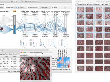
From materials science and earth system modeling to quantum information science and cybersecurity, experts in many fields run simulations and conduct experiments to collect the abundance of data necessary for scientific progress.

Five researchers at the Department of Energy’s Oak Ridge National Laboratory have been named ORNL Corporate Fellows in recognition of significant career accomplishments and continued leadership in their scientific fields.
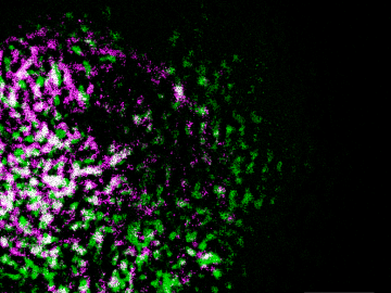
Oak Ridge National Laboratory researchers have built a novel microscope that provides a “chemical lens” for viewing biological systems including cell membranes and biofilms.
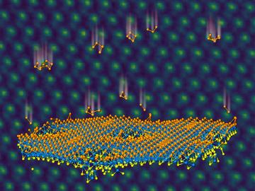
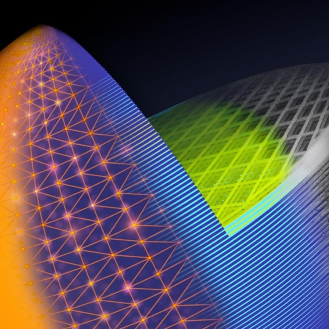
An ORNL team used a simple process to implant atoms precisely into the top layers of ultra-thin crystals, yielding two-sided structures with different chemical compositions.