Scientific Achievement
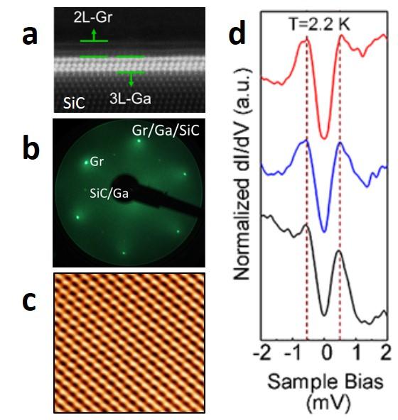
A new approach to stabilizing atomically thin crystalline metals (Ga, In, Sn) at the interface of silicon carbide and epitaxial graphene.
Significance and Impact
This work demonstrates a new strategy to create air-stable, wafer-scale 2D metals that are not prone to interfacial interactions for novel quantum and information sciences beyond traditional semiconductor approaches.
Research Details
- Defect engineering and interface templating enable intercalation and crystallization of metals at a thermodynamically defined number of atomic layers.
- Scanning tunneling microscopy (STM) reveals the structure, superconductive critical temperature, and critical field.
- Low-energy electron diffraction (LEED) pattern determines the lattice registration relations.
N. Briggs, B. Bersch, Y. Wang, J. Jiang, R. J. Koch, N. Nayir, K. Wang, M. Kolmer, W. Ko, A. De La Fuente Duran, S. Subramanian, C. Dong, J. Shallenberger, M. Fu, Q. Zou, Y-W. Chuang, Z. Gai, A-P. Li, A. Bostwick, C. Jozwiak, C-Z. Chang, E. Rotenberg, J. Zhu, A. C. T. van Duin, V. Crespi, and J. A. Robinson, "Atomically Thin Half-van der Waals Metals Enabled by Confinement Heteroepitaxy," Nature Mater. (2020). DOI: 10.1038/s41563-020-0631-x


