Scientific Achievement
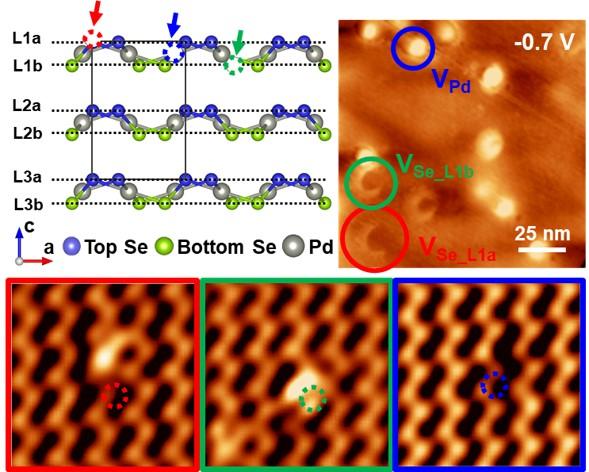
The screened Coulomb interaction between an STM tip and charged single atom vacancy creates large-scale features around individual defects. This effect magnifies sublayer defects to make them visible.
Significance and Impact
By gating the probe, STM and AFM can be used to characterize sublayer atomic defects in a nondestructive way.
Research Details
Scanning tunneling microscopy (STM) and spectroscopy (STS) were combined with density functional theory (DFT) calculations to identify the atomic and electronic structures of pristine and various intrinsic vacancy defects in PdSe2.
Vacancies are charged by tip-gating, resulting in a protrusion around Palladium vacancies (VPd) and crater-like features around Selenium vacancies (Vse).
M. Fu, L. Liang, Q. Zou, G. D. Nguyen, K. Xiao, A.-P. Li, J. Kang, Z. Wu, and Z. Gai, "Defects in Highly Anisotroic Transition-Metal Dichalcogenide PdSe2," J. Phys. Chem. Lett. (2019). DOI: 10.1021/acs.jpclett.9b03312


