Bio
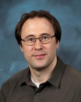
Dr. Nelson is a TEM & STEM Electron Microscopist at ORNL since 2017. He received a BS in Electrical Engineering from the University of Virginia with a work-study internship in metrology at a Micron Inc. DRAM Fab. Following an interest in electronic materials he received a PhD in Materials Science from U. Michigan and was a post-doctoral researcher at the U.C. Berkeley / LBNL, specializing in (S)TEM characterization of complex oxides. His research expertise includes electronic materials, in-situ electrical biasing, electronic hardware and circuit design. This includes significant software development in hardware controls/detection and (S)TEM data analysis including raster distortion correction, atom finding, symmetry mapping, time dynamics, and AI Autoencoders (see github link).
Professional Experience
2017-Present: Materials Scientist Electron Microscopy, Oak Ridge National Laboratory
2012-2016: Postdoctoral Researcher, University of California Berkeley / National Center for Electron Microscopy, Laurence Berkeley National Laboratory
2005-2012: Graduate Researcher, Materials Science and Engineering, University of Michigan
2004,2005: Intern, Metrology Dept. Micron Inc., Manassas VA
2001-2004: Undergraduate Researcher, Materials Science and Engineering, University of Virginia
1999,2000: High School Summer Intern, Naval Research Laboratory
Education
2011: Ph.D. Material Science University of Michigan
2005: B.S. Electrical Engineering University of Virginia

