Updated software improves slicing for large-format 3D printing

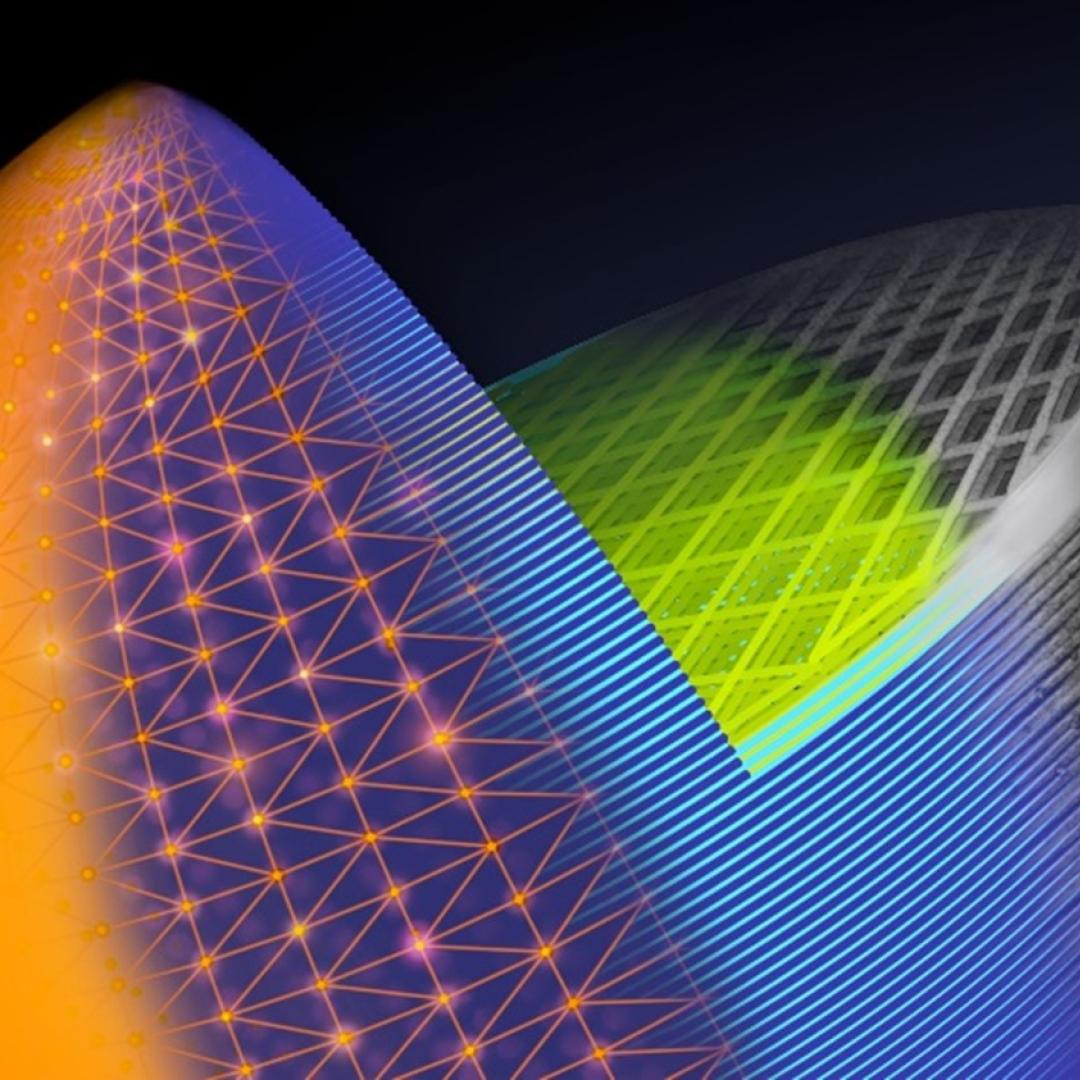
An Oak Ridge National Laboratory–led team has learned how to engineer tiny pores embellished with distinct edge structures inside atomically-thin two-dimensional, or 2D, crystals. The 2D crystals are envisioned as stackable building blocks for ultrathin electronics and other advance...

It may take a village to raise a child, according to the old proverb, but it takes an entire team of highly trained scientists and engineers to install and operate a state-of-the-art, exceptionally complex ion microprobe. Just ask Julie Smith, a nuclear security scientist at the Depa...

A scientific team led by the Department of Energy’s Oak Ridge National Laboratory has found a new way to take the local temperature of a material from an area about a billionth of a meter wide, or approximately 100,000 times thinner than a human hair. This discove...

Material surfaces and interfaces may appear flat and void of texture to the naked eye, but a view from the nanoscale reveals an intricate tapestry of atomic patterns that control the reactions between the material and its environment. Electron microscopy allows researchers to probe...