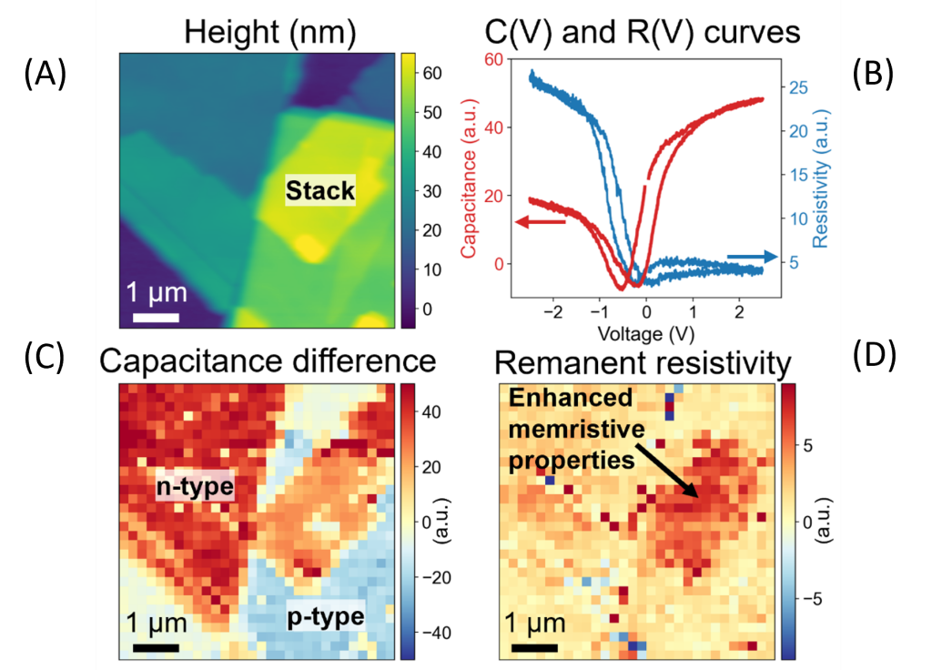
(A) AFM height image of PdSe2 nanosheets and stack.
(B) Simultaneously measured C(V) and R(V) curves.
(C) Capacitance difference between charge accumulation and inversion calculated from C(V) curves.
(D) Remanent resistivity obtained from R(V) related to memristive properties.
(B) Simultaneously measured C(V) and R(V) curves.
(C) Capacitance difference between charge accumulation and inversion calculated from C(V) curves.
(D) Remanent resistivity obtained from R(V) related to memristive properties.
Scientific Achievement
Nanoscale electrical probing reveals enhanced memcapacitive and memristive properties in stacked nanosheets of PdSe2.
Significance and Impact
Switchable electrical states are fundamental to energy-efficient neuromorphic hardware elements
Research Details
- Demonstrated nanoscale electrical characterization of semiconductors based on atomic force microscopy.
- Enhanced resistive and capacitive switching was found in stacked PdSe2 nanosheets due to trapped charge carriers at the interface. Unexpected local p-type semiconducting behavior was detected that provides further tunability.
Neumayer, et al., ACS Applied Materials & Interfaces 16, 3665 (2024). DOI: 10.1021/acsami.3c14427
Work performed at the Center for Nanophase Materials Sciences